National Semiconductor MM-57100N
Inicio › Ordenadores › Microprocessors
Microprocessors
Máquinas (61–120 de 182)
Intel 8088
Ficha técnica
Historia
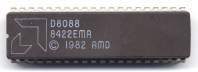
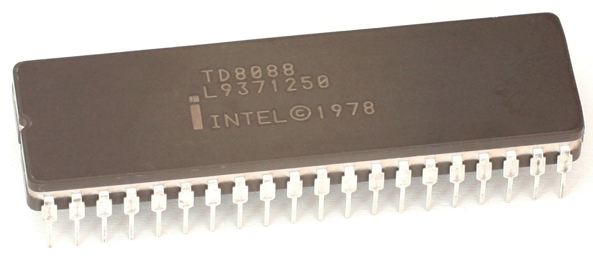
The Intel 8088 (eighty-eighty-eight, also called iAPX 88) microprocessor is a variant of the Intel 8086. Introduced on June 1, 1979, the 8088 had an eight-bit external data bus instead of the 16-bit bus of the 8086. The 16-bit registers and the one megabyte address range were unchanged, however. In fact, according to the Intel documentation, the 8086 and 8088 have the same execution unit (EU)—only the bus interface unit (BIU) is different. The original IBM PC was based on the 8088, as were its clones.
Motorola 68000
Ficha técnica
Historia
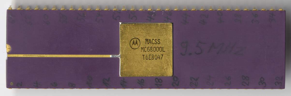
The Motorola 68000 (sixty-eight-thousand; also called the m68k or Motorola 68k, sixty-eight-kay) is a 16/32-bit CISC microprocessor, introduced in 1979 by Motorola Semiconductor Products Sector. The first member of Motorolas family of 16- and 32-bit processors. Successor to the 6809 and followed by the 68010. The 68000 has 32-bit registers but only a 16-bit ALU and external data bus. It has 24-bit addressing and a linear address space. Addresses are computed as 32 bit, but the top 8 bits are cut to fit the address bus into a 64-pin package (address and data share a bus in the 40 pin packages of the 8086). The 68000 has sixteen 32-bit registers, split into data and address registers. Like many other CPUs of its generation, it can fetch the next instruction during execution (2 stage pipeline). The 68000 was used in many workstations, notably early Sun-2 machines, and home computers like Apple Macintosh, Commodore Amiga and Atari ST series. Variants of the 68000 include the 68HC000 (a low-power HCMOS implementation) and the 68008 (an eight-bit data bus version used in the Sinclair QL). The 68EC000 is a 68000 with selectable 8 or 16 bit data bus and A0.
Motorola 68000
Ficha técnica
Historia
The Motorola 68000 (sixty-eight-thousand; also called the m68k or Motorola 68k, sixty-eight-kay) is a 16/32-bit CISC microprocessor, introduced in 1979 by Motorola Semiconductor Products Sector.
Zilog Z8000
Ficha técnica
Historia
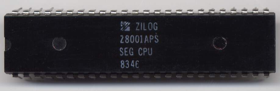
Zilog Z8000 is a family of 16-bit microprocessors introduced in 1979 between the Intel 8086 and the Motorola 68000. The series has been designed by Masatoshi Shima and produced by Zilog and second sources AMD, SGS and Hitachi from 1979 until 1995. Since 1995, the CPU series continues to live and still is in production by Zilog in a pin-compatible CMOS release called the Z16C00 series (with the Z16C01 as the equivalent of Z8001 and the Z16C02 as the equivalent of Z8002). There are 4 slightly different Z8000 versions: Z8001: large memory version, can address up to 8 MB (divided into 128 segments up to 64 KB each) Z8002: small memory version, can address 64 KB Z8003: same as the Z8001 with added virtual memory support Z8004: same as the Z8002 with added virtual memory support The Z8000 series introduced a number of attractive new features from the mini-computer and mainframe worlds: Regular general-purpose register file (16 16-bit registers that could be used as accumulators, address registers, index registers or stackpointers) Separation of Normal and System modes (also known as User and Supervisor modes) for enhancing system integrity Large address space (8Mb) First commercial Memory management facility (Z8010 Z-MMU) Extended Processing Architecture (EPA) allowing co-processing in an efficient parallel fashion The Z8000 processor also had some drawbacks as compared to its close rival, the Motorola 68000: Segmented addressing: maximum segment size of 64Kb which complicates the addressing of very large data structures Delayed introduction due to tecnical problems Limited support (very limited software base, limited hardware support) Although initially the Z8000 got some acceptance and was widely recognised to have a very elegant and user-friendly architecture, it became quickly surpassed by the Motorola 68000 and the Intel 80286 in the commercial domain. In safe-critical environments however the processor apparently continued to play an important role.
General Instruments AY-3-8610
Ficha técnica
Historia
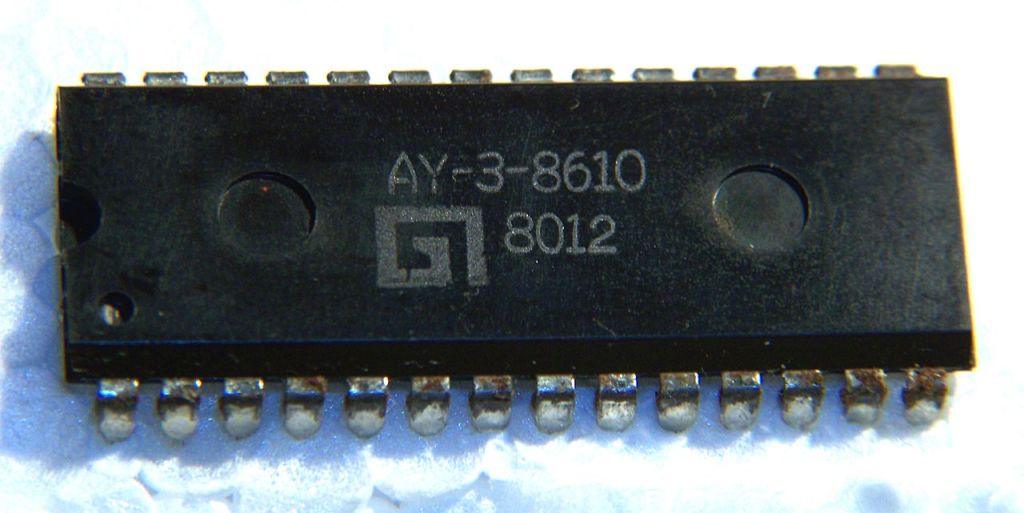
The AY-3-8610 was a major update from General Instruments. It played more games (10), like basketball or hockey, with higher-quality graphics. It was nicknamed Superstar by GI. It was in black and white, although it was possible to add color by using an additional AY-3-8615 chip. Prior to producing the 8610, GI created the AY-3-8600. The pin configuration was the same as the 8610, but it was missing the two rifle/target games, bringing the total number of games down to 8.
Características
Improved 8600 with 2 target shooting games


AMD 80286
Ficha técnica
Historia
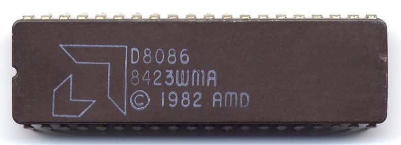
AMD started in the x86 business as a second-source manufacturer for Intels chip designs. IBM demanded all suppliers have a second manufacturing source, and Intel had to license another company to secure the IBM PC contract. The AMD 80286 was a result of this contract. The AMD 80286 was in reality Intel-designed all the way, pin and instruction compatible, based upon Intels microcode.
Intel 80186-188
Ficha técnica
Historia
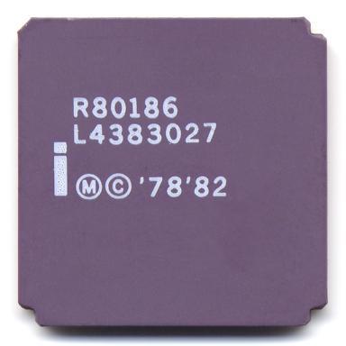
The 80186 microprocessor was developed by Intel in 1982. It is an improved 8086 with several common support functions built in: clock generator, system controller, interrupt controller, DMA controller, and timer/counter. It also added 8 new instructions and executes instructions faster than the 8086. As with the 8086, it has a 16-bit external bus and is also available as the 80188, with an 8-bit external data bus. The initial clock rate of the 80186 and 80188 was 6 MHz. They were, and still are, generally used as embedded processors but also as the CPU of few personal computers: The Mindset graphics computer, a very advanced computer for the time. It had proprietary chips that enhanced and sped up the graphics. The original Gateway Handbook, a small subnotebook computer. The Telenova Compis, a Swedish school computer. The Tandy 2000, a somewhat PC-compatible workstation featuring particularly advanced graphics for its time. In 1987 Intel announced the second generation of the 80186 family: the 80C186/C188. The 80186 was redesigned as a static, stand-alone module known as the 80C186 Modular Core and is pin compatible with the 80186 family, while adding an enhanced feature set. The high-performance CHMOS III process allowed the 80C186 to run at twice the clock rate of the NMOS 80186, while consuming less than one-fourth the power. In 1991 the 80C186 Modular Core family was again extended with the introduction of the 80C186XL. The 80C186XL/C188XL is a higher performance, lower power replacement for the 80C186/C188.
Intel 80286
Ficha técnica
Historia
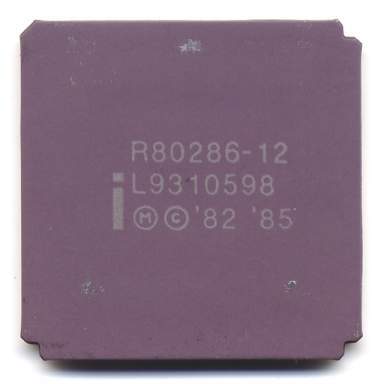
The 80286 was introduced by Intel on February 1, 1982. As the 80186/80188 CPUs were not really significant to personal computing, the 80286 was Intels next step processor for micro computers. Intel added four more address lines to the 8086/80186 design. The 8086, 8088, 80186, and 80188 all contained 20 address lines, giving these processors one megabyte of addressibility (2^20 = 1MB). The 80286, with its 24 address lines, gives 16 megabytes of addressibility (2^24 = 16 MB). The most substantial difference between the 80286 and the 8086/8088 is the addition of a protected mode. In protected mode, segment registers became pointers into a table of memory descriptors rather than being a direct part of the address. Among other things, protected mode allows safe execution of multiple programs at once by protecting each program in memory. DOS normally operates in real mode, in which segment registers act just as they do in the 8086/8088. Protected mode is used by Microsoft Windows, IBMs OS/2 and UNIX. (For an introduction to protected mode please refer to this source) The 80286 is a much more powerful CPU than the 8086, offering 3-6 times the performance of it. The 6 MHz 80286 is the CPU of the IBM AT (Advanced Technology), which also introduced a 16-bit motherboard and 16-bit expansion bus to the PC world. The IBM AT was introduced in 1985 - three years after introduction of the 80286. With the 80286, the first chipsets were introduced. The computer chipset is a set of chips that replaced dozens of other peripheral chips while maintaining identical functionality. Chips and Technologies became one of the first popular chipset companies. Intel second-sourced the 80286 to ensure an adequate supply of chips to the computer industry. AMD, IBM, and Harris were known to produce 80286 chips as OEM products; while Siemens, Fujitsu, and Kruger either cloned it or were also second-sources. Between these various manufacturers, the 80286 was offered in speeds ranging from 6 MHz to 25 MHz: Intel: 6 - 12.5 MHz Siemens: 8 - 16 MHz AMD: 8 - 20 MHz Harris: 10 - 25 MHz The 80286 was typically made in 3 package versions, each with 68 contacts: a PGA-, CLCC- and a PLCC-package. Its successor is the 386. The 286 was widely used in IBM PC compatible computers during the mid to late 1980s.
Intel 80287
Ficha técnica
Historia
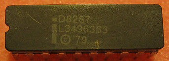
Mathematical coprocessors for the 80286
Ricoh 2A03
Ficha técnica
Historia
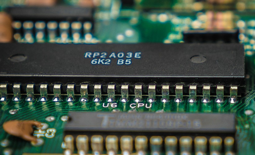
The Ricoh 2A03 or RP2A03 (NTSC version) / Ricoh 2A07 or RP2A07 (PAL version) is an 8-bit microprocessor manufactured by Ricoh for the Nintendo Entertainment System video game console. It was also used as a sound chip and secondary CPU by Nintendos arcade games Punch-Out!! and Donkey Kong 3.
MOS Technology 6510
Ficha técnica
Historia
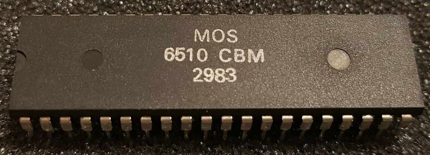
This CPU is built in my Commodore C64 computer from 1983. The MOS6510 is a 6502 with an additional 6 Bit bidirectional I/O Port. (The pre-release spec of the 6510 mentions a 8Bit port and since there was never a official release specification of the 6510 all literature copied the version with the 8Bit wide Port. Maybe it was planned, but in the end the 6510 got only an additional 6Bit.) The 6510 (and the 6502) can run also at 2Mhz. So does the 8502 version in the C128 Computer and the 6502 in the 1571 Disk Drive. The 6510 that was built in the C64 ran at 1 Mhz, so it was compatible to the VIC2 Videochip.
NEC D779C
Ficha técnica
Historia
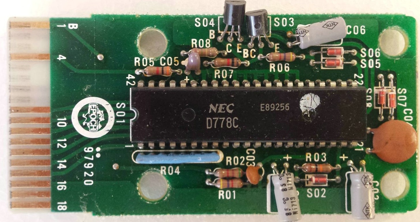
NEC were known for cloning other CPUS; The D780C was a clone of the Z80. The D779C appears to be more a system chip, like a microcontroller. It may be a custom-made Z80 MCU with certain features removed for cost. Unfortunately, as there is no information available I can not confirm this, so this is a best educated guess.
Características
Soundic Soundvision SD-200. There is three types of models: the SD-200, the SD-270 and the SD-290 but all have the same main chip: a NEC uPD779C-300.
The D779C is very similar to the chips inside the ECV cartridges but there is a major difference, the D779C is programmable compared to the D774C, D777C and D778C.
MOS Technology 7501
Ficha técnica
Historia
The 7501 variant of the 6510 was used in Commodores C16, C116 and Plus/4 home computers, and the 2 MHz-capable 8502 variant was used in the Commodore C128. All these CPUs are opcode compatible (including undocumented opcodes).
ARM Acorn RISC Machine
Ficha técnica
Historia
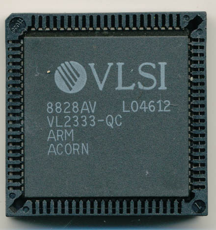
ARM, previously Advanced RISC Machine, originally Acorn RISC Machine, is a family of reduced instruction set computing (RISC) architectures for computer processors, configured for various environments. The British computer manufacturer Acorn Computers first developed the Acorn RISC Machine architecture (ARM) in the 1980s to use in its personal computers.
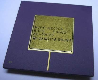
MIPS R2000
Ficha técnica
Historia
MIPS (Microprocessor without interlocked pipeline stages) is a RISC microprocessor architecture developed by MIPS Computer Systems Inc in the early eighties. MIPS processors were used in high-end servers from Siemens and DEC and especially in SGIs computer product line, and have found broad application in embedded systems, Windows CE devices, and Cisco routers. The Nintendo 64 and Sony PlayStation 2 consoles also use MIPS processors. The architecture was very successful, about one third of all RISC chips produced in mid 1990s were MIPS based designs. In 1999 the ARM/StrongARM architecture took over rather decisively in thanks to cell phone and PDA usage.
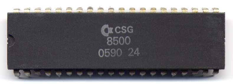
MOS Technology 8500
Ficha técnica
Historia
In 1985 MOS produced the 8500, an HMOS version of the 6510. Other than the process change, it is virtually identical to the NMOS version of the 6510. The 8500 was originally designed for use in the modernised C64, the C64C. However in 1985, limited quantities of 8500s were found on older NMOS based C64s. It finally made its official debut in 1987, appearing in a motherboard using the new 85xx HMOS chipset. The MOS 8502 was also based on the MOS 6510 that was used in the Commodore 64. The 8502 added the ability to run at a double (2.048 MHz) clock rate, in addition to the standard 1.024 MHz rate used by the Commodore 64. The pinout is a little bit different from the 6510. The 8502 has an extra I/O-pin and lacks the PHI2-pin that the 6510 had. The 7501/8501 variant of the 6510 was used in Commodores C16, C116 and Plus/4 home computers, and the 2 MHz-capable 8502 variant was used in the Commodore C128. All these CPUs are opcode compatible (including undocumented opcodes).
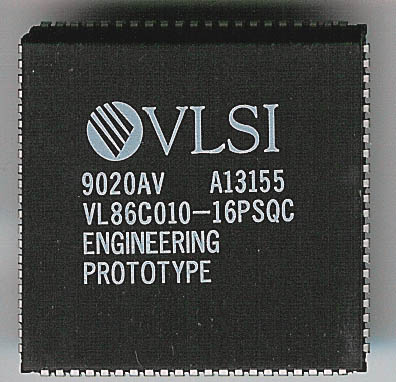
ARM2
Ficha técnica
Historia
Introduced in 1986, the ARM2 is a reimplementation of the ARM1 on a smaller process along with the addition of a number of additional enhancements. The ARM2 was capable of exceeding 10 MIPS when not bottlenecked by memory with an average of around 6 MIPS. Unlike the ARM1 which was predominantly a research project, the ARM2 became the first commercially successful ARM microprocessor. The ARM2 was designed to work as an embedded controller or a coprocessor or as a stand-alone microprocessor system. The Acorn Archimedes family of personal computers was built using the ARM2 along with a number of fully custom support chips that were also designed by Acorn Computer.
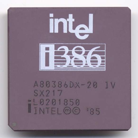
Intel 386 DX
Ficha técnica
Historia
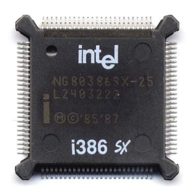
The 386 was the successor to the 80286 processor and the first Intel processor with 32-bit data and address busses. It can address four gigabytes (2^32 bytes) of memory - however, 16 megabytes is a typical maximum in IBM PCs. The 386 allows multiple application programs to run at the same time (when running under 386-specific operating systems) using protected mode. The first IBM compatible to use the 386 was the Compaq 386, before IBM used it in high-end models of their PS/2 series. With the 386, Intel introduced the DX - SX naming system. DX stands for Double-word eXternal, SX for Single-word eXternal. The SX versions therefore are lower-speed version of the 386(DX). They use a 16-bit data bus instead of a 32-bit data bus.
Intel 386 SX
Ficha técnica
Historia
With the 386, Intel introduced the DX - SX naming system. DX stands for Double-word eXternal, SX for Single-word eXternal. The SX versions therefore are lower-speed version of the 386(DX). They use a 16-bit data bus instead of a 32-bit data bus.
Intel 387 DX
Ficha técnica
Historia
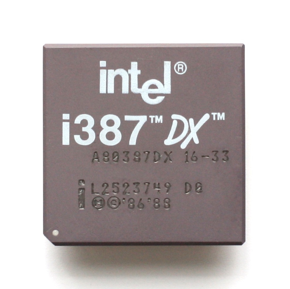
Mathematical coprocessors for the i386SX
Intel 487SX
Ficha técnica
Historia
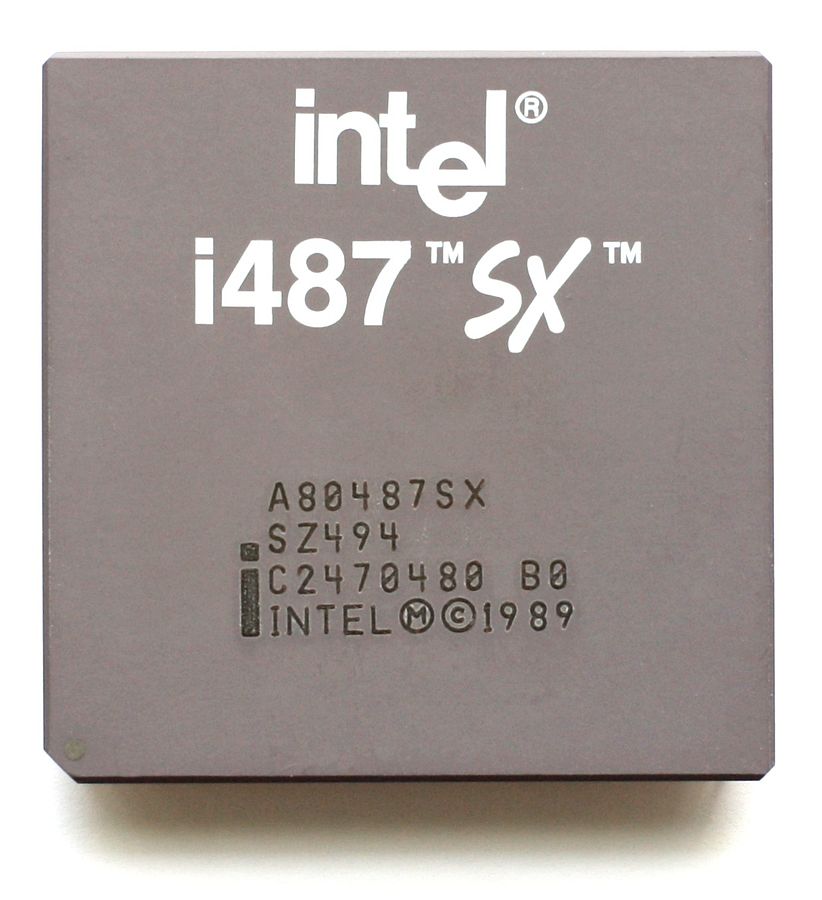
The first version was an 80486DX with disabled math coprocessor in the chip and different pin configuration. If the user needed math coprocessor capabilities, he must add 487SX which was actually a 486DX with different pin configuration to prevent the user from installing a 486DX instead of 487SX, so with this configuration 486SX+487SX you had 2 identical CPUs with only 1 effectively turned on
MIPS R3000
Ficha técnica
Historia
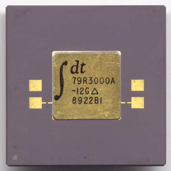
R3000, the first successful MIPS design in the marketplace with more than 1 million processors made. The R3000 was used in high-end UNIX computers by Siemens and DEC and in the Silicon Graphics SGI Personal IRIS 4D/20 graphic workstations. On this machines 3D sequences for movies like The Abyss, Jurrasic Park or Terminator 2 were rendered. The R3000 has an interface to handle 3 coprocessors. Each coprocessor has a flag line connected with the CPU that can be tested and a conditional branch executed dependent on its value. Coprocessor instructions can be executed directly from the instruction stream. Coprocessor 0 (CP0) is incorporated on the CPU chip and supports the virtual memory system and exception handling. It is also referred to as the System Control Coprocessor. CP1 is reserved for the floating point coprocessor. An FPU is mandatory for most R3000 systems. CP2 is available for specific implementations and is often used to accelerate memory access by connecting it to an R3020 memory buffer or an R3220 read/write buffer chip. Later versions of the R3000 (R3000A) had built in memory buffer circuitry.
Cyrix 387 DX
Ficha técnica
Historia
The predecessor of the CX-83D87. The Cyrix 387DX was soon replaced by the much more advanced CX-83D87
Cyrix 487 DLC
Ficha técnica
Historia
The 487DLC is a math processor for the Cyrix 486 DLC series of 386DX replacement processors. The Cx487DLC is an OEM only chip and has not been sold separately.
Cyrix Fasmath CX-83D87
Ficha técnica
Historia
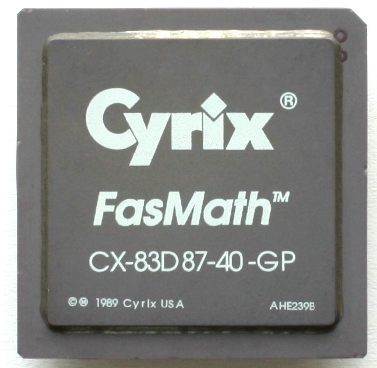
The CX-83D87 was introduced in 1989. It is the fastest 387-compatible coprocessor and provides up to 50% more performance than the Intel 387DX. The 83D87 also offers the most accurate transcendental functions of all coprocessors. It is the 387 clone with the highest degree of compatibility to the Intel 387DX. Unlike the Intel 387DX, the 83D87 (and all other 387-compatible chips as well) does not support asynchronous operation of CPU and coprocessor. To reduce power consumption the 83D87 features advanced power saving features. Those portions of the coprocessor that are not needed are automatically shut down. If no coprocessor instructions are being executed, all parts except the bus interface unit are shut down.
DMG-CPU B Game Boy
Ficha técnica
Historia
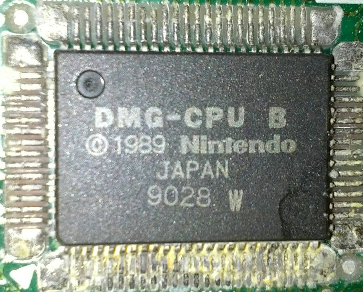
Nintendo Game Boy, based on Z80
Intel 486 DX
Ficha técnica
Historia
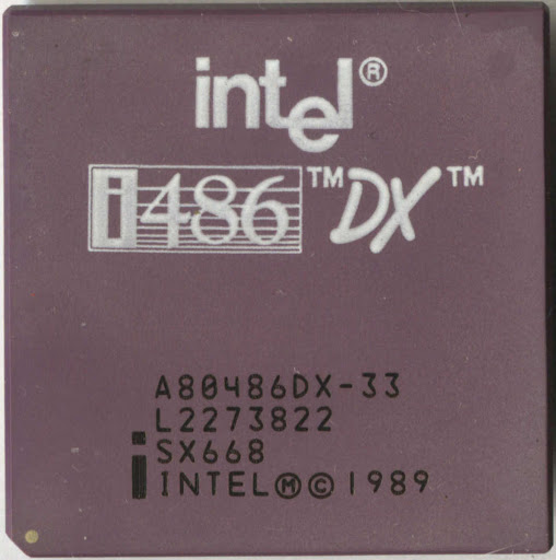
The 486 is very similar to its predecessor, the 386. Main differences are an optimised instruction set, an on-chip unified instruction and data cache, an optional on-chip floating-point unit (FPU), and an enhanced bus interface unit. These improvements yield a rough doubling in performance over an 386 at the same clock rate. There are several suffixes and variants including: 486SX - 486 with its FPU disabled 486DX - 486 with a working FPU 486DX-2 - runs at twice the external clock rate 486SL - 486DX with power conservation circuitry 486SL-NM - 486SX with power conservation circuitry 487 - 486DX with slightly different pinout for use in 486SX systems as FPU OverDrive - 486DX-2 with slightly different pinout for use in 486SX systems RapidCAD - 486DX in a special package with a companion FPU dummy package for use in 386 systems 486DLC - mix version by some manufacturers, featuring a 486 instruction set and a 386-compatible pinout The 486 processor has been licensed or reverse engineered by other companies such as IBM, AMD and Cyrix. Some manufacturers made hybrid 386/486 CPUs (Cxrix Cx486DLC, Texas Instruments TX486DLC), having a 486 instruction set and a 386-compatible pinout.
AMD Am486DX
Ficha técnica
Historia
The Am486 is a 80486-class processors produced by AMD in the 1990s. Intel beat AMD to market by nearly four years, but AMD priced its 40 MHz 486 at or below Intels price for a 33 MHz chip, offering about 20% better performance for the same price. Early AMD 486 chips were drop-in replacements for their Intel counterparts, but later AMD clock-doubled 486s ran at 3.3 volts instead of Intels 5 volts, which limited their suitability as upgrade chips until third-party voltage adapters appeared on the market. While the Am386 was primarily used by small computer manufacturers, the Am486DX, DX2, and SX2 chips gained acceptance among larger computer manufactuers, expecially Acer and Compaq, in the 1994 time frame. AMDs higher clocked 486 chips provided superior performance to many of the early Pentium chips, especially the 60 and 66 MHz launch products. While equivalent Intel 80486DX4 chips were priced high and required a minor socket modification, AMD priced low. Intels DX4 chips had twice the cache of the AMD chips, giving them a slight performance edge, but AMDs DX4-100 usually cost less than Intels DX2-66.
AMD Am386
Ficha técnica
Historia
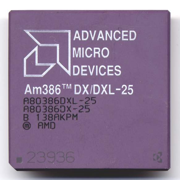
The Am386 CPU was released by AMD in 1991. A 100%-compatible clone of the Intel 80386 design, it sold millions of units and positioned AMD as a legitimate competitor to Intel, rather than just a second source for Intels x86 CPUs. While the CPU was essentially ready to be released prior to 1991, Intel kept it tied up in court. AMD had previously been a second-source manufacturer of Intels designs, and AMDs interpretation of the contract was that it covered all of them. Intel, however, claimed that the contract only covered the 80286 and prior processors. After a few years in the courtrooms, AMD finally won the case and the right to sell their Am386. This paved the way for competition in the CPU market and thus lowered the cost of owning a PC.

AMD Am386SX
Ficha técnica
Historia
In 1991 AMD introduced advanced versions of the 386SX processor - not a second source production of the Intel chip, but a reverse engineered pin compatible version. In fact, it was AMDs entry in the x86 market other than as a second source for Intel. AMD 386SX processors were available at faster clock speeds at the time they were introduced and still cheaper than the Intel 386SX. Produced in 0.8 mm technology and using a static core their clock speed could be dropped down to 0 MHz, consuming just some mWatts. Power consumption was up to 35% lower than with Intels design and even lower than the 386SLs, making the AMD 386SX the ideal chip for both desktop and mobile computers. The SXL versions featured advanced power management functions and used even less power
ARM3
Ficha técnica
Historia
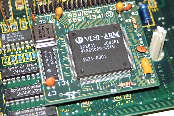
The next iteration of the ARM processor came in the form of the ARM3. Offering a 4KiB unified cache, plus increased clock speeds (usually 25MHz, although some 33MHz parts exist), it was compatible enough for a carrier board to be designed to plug in where an ARM2 used to be, giving an older machine an instant resurrection as something new. The ARM3 adds the SWP instruction, which is a atomic instruction to swap data between registers and memory and is guaranteed not to be interrupted (unlike the corresponding LDR/STR sequence) so it may be used for system semaphores. The first machine to use the ARM3 onboard was Acorns A5000 (1991) and the A4 laptop (1992, although the A5000 design is derived from the A4!). Clocking at 25MHz (24MHz for the A4), the machine offers around 13.5 MIPS, which is about what youd expect for the difference in clock speed. The Alpha versions of the A5000 (clocked at 33MHz) offer nearly 18 MIPS. By way of comparison, an Intel 80386DX clocking 25MHz provides 8.5 MIPS, while the higher power (and phenomenally expensive in its day) 80486(any version) generally offered around 20 MIPS at 25MHz.
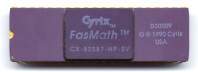
Cyrix FasMath For 286
Ficha técnica
Historia
This 80287-compatible chip was developed from the Cyrix 83D87 and has been available since 1991. It complies completely with the IEEE-754 standard for floating-point arithmetic and features nearly total compatibility with Intels coprocessors, including implementation of the full Intel 80387 instruction set. It implements the transcendental functions with the same degree of accuracy and the superior speed of the Cyrix 83D87. This makes the Cyrix 82S87 the fastest and most accurate 287 compatible coprocessor available. Documentation by Cyrix rates the 82S87 at 730 kWhets/sec for a 12.5 MHz system, while the Intel 287XL performs only 552 kWhets/sec. 82S87 chips manufactured after 1991 use the internals of the Cyrix 387+, which succeeds the original 83D87.
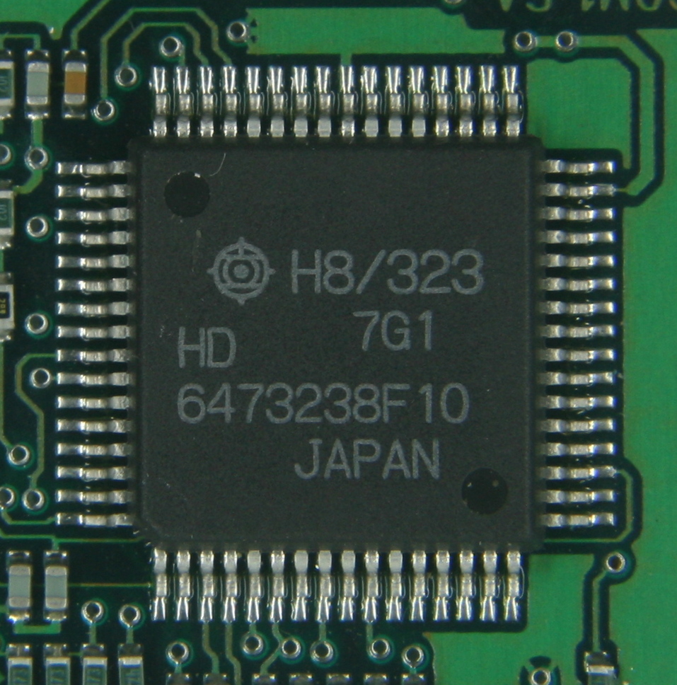
Hitachi H8
Ficha técnica
Historia
H8 is the name of a large family of 8-bit, 16-bit and 32-bit microcontrollers made by Renesas Technology, originating in the early 1990s within Hitachi Semiconductor.
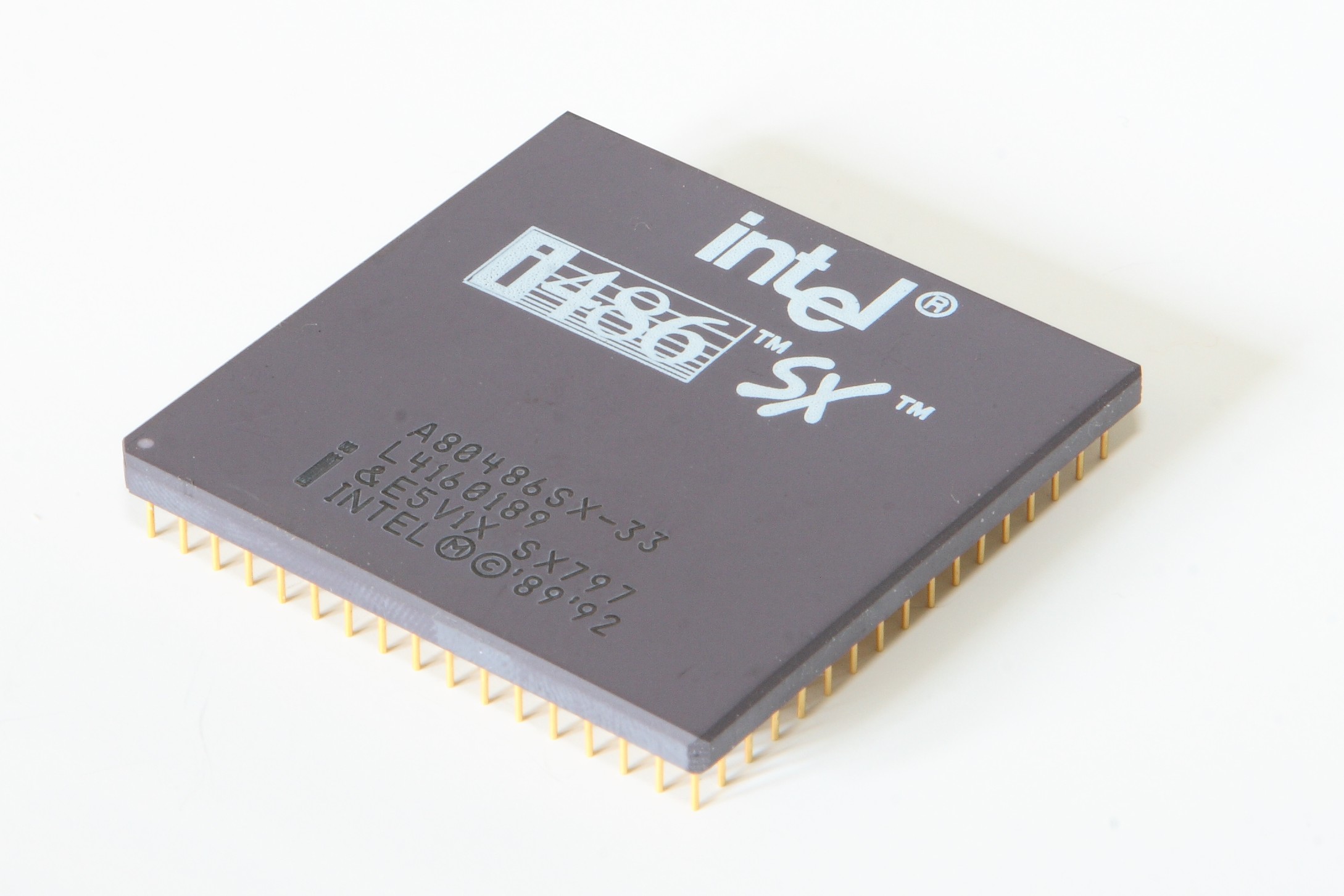
Intel 486SX
Ficha técnica
Historia
Identical in design to 486DX but without a math coprocessor. The first version was an 80486DX with disabled math coprocessor in the chip and different pin configuration. If the user needed math coprocessor capabilities, he must add 487SX which was actually a 486DX with different pin configuration to prevent the user from installing a 486DX instead of 487SX, so with this configuration 486SX+487SX you had 2 identical CPUs with only 1 effectively turned on
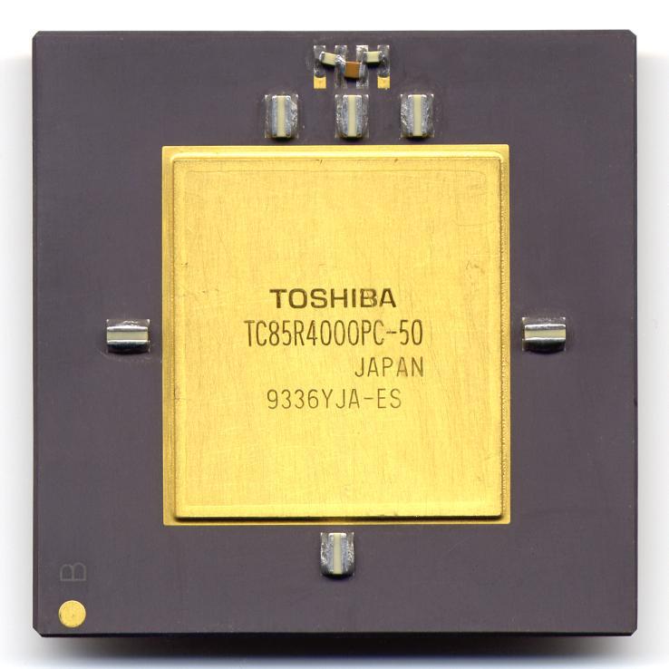
MIPS R4000
Ficha técnica
Historia
The MIPS R4000 series, released in 1991, extended the MIPS instruction set to a full 64-bit architecture and moved the FPU onto the main die to create a single-chip system. The design was so important to SGI, at the time MIPS major customer, that SGI bought the company in 1992. The R4x00 processors have been available and used in different versions. PC (as in R4000PC) denotes primary cache only and SC denotes secondary cache. The MC versions contain special support for cache architectures in multiprocessor systems. R4000 processors where used in many Silicon Graphics computers, e.g. the Indigo workstations and Crimson servers.
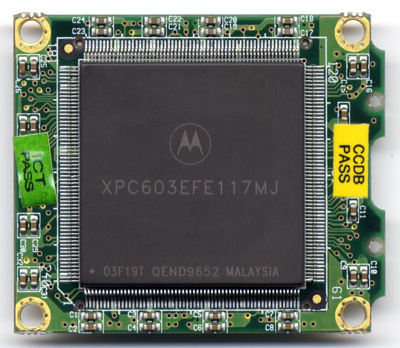
Motorola PowerPC 603
Ficha técnica
Historia
PowerPC is a RISC microprocessor architecture created by the 1991 Apple-IBM-Motorola alliance (AIM). Power (Performance Optimization With Enhanced RISC) and was adopted from IBMs POWER architecture from their RS/6000 series. The PowerPC is designed along RISC principles, and allows for a superscalar implementation. Versions of the design exist in both 32-bit and 64-bit implementations. Starting with the basic POWER specification, the PowerPC added: big or little-endian modes (requiring a reset) single-precision floating point in addition to double-precision additional floating point instructions at the behest of Apple a complete 64-bit specification, which is backward compatible with the 32-bit mode removal of some of the more esoteric POWER instructions, which are emulated in microcode The first single-chip implementation of the design was the MCP601 and released in Apples PowerMac in March 1994
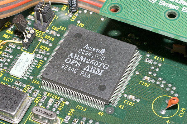
ARM250
Ficha técnica
Historia
Late in 1992, Acorn launched new budget machines - two more in the A3000 range (A3010 and A3020) and an A4000 which was a business oriented mini-A5000. The principal difference was a reduction of board complexity with Acorn/ARMs first foray into SoC (System-on-Chip) design in which the main components of the ARM chipset (ARM, MEMC, VIDC, IOC) were coupled together in one piece of silicon. As it happens, initial supply problems meant that early machines did not have an ARM250 but instead a mezzanine board containing the individual chips. An ARM250 is more or less an ARM3 without the cache, so it ought to be detectable by the lack of a cache but the support of SWP, though the mezzanine version may just behave like a marginally faster ARM2 machine. Clocking 12MHz, this SoC delivers around 7 MIPS.
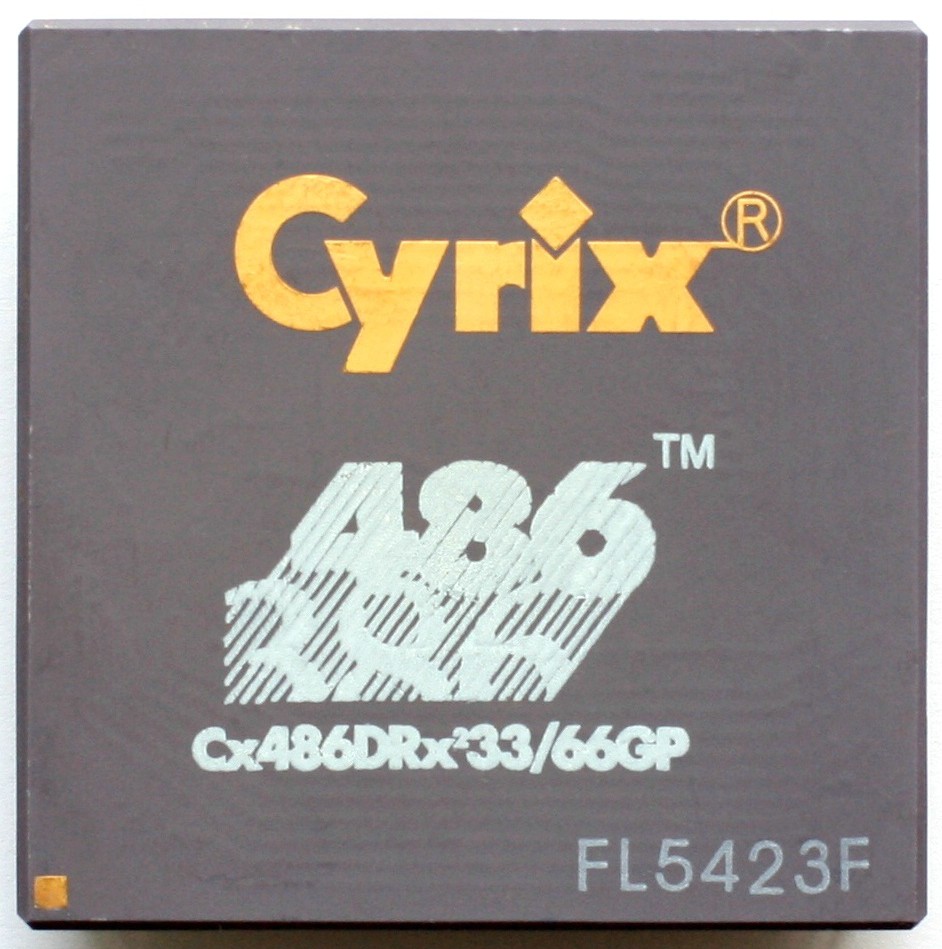
Cyrix 486
Ficha técnica
Historia
The Cyrix 486DLC is pin compatible to the Intel i386DX. While the internals of the 486DLC are roughly equivalent to those in the i486SX, the bus interface is identical to that of the Intel 386DX, respectively to allow easy replacement of the Intel CPUs by the Cyrix chips. The overall execution speed is about same as with an i486SX, but if you add a matching Cyrix FPU, e.g. a Cyrix 83D87, the speed is about 50% faster than an i486DX running at the same frequency.
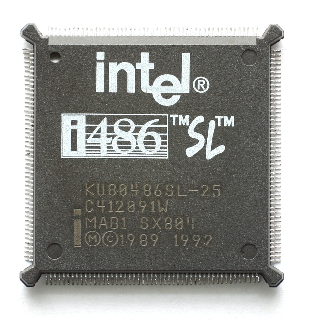
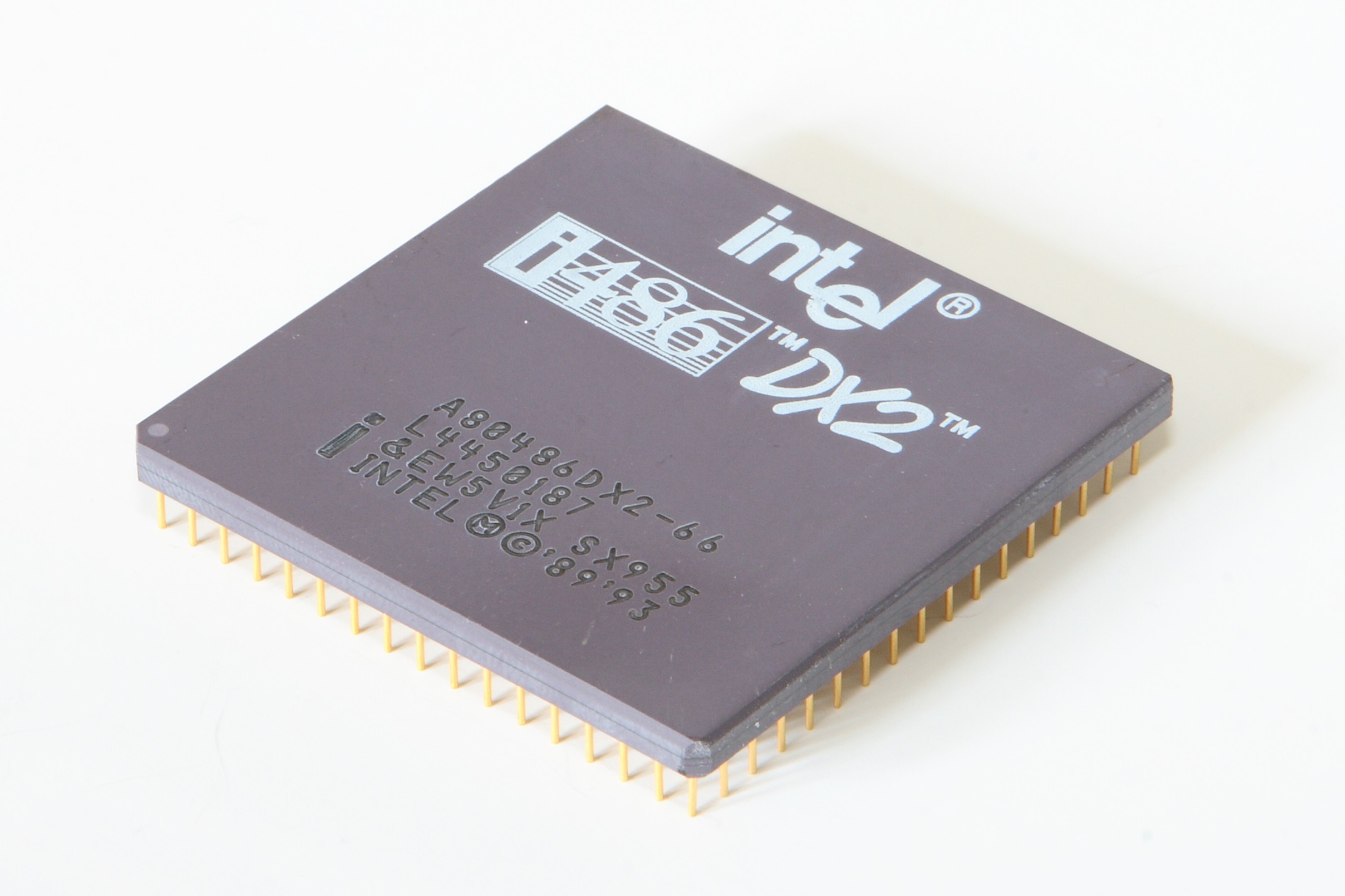
Intel 486DX2
Ficha técnica
Historia
486DX-2 - runs at twice the external clock rate
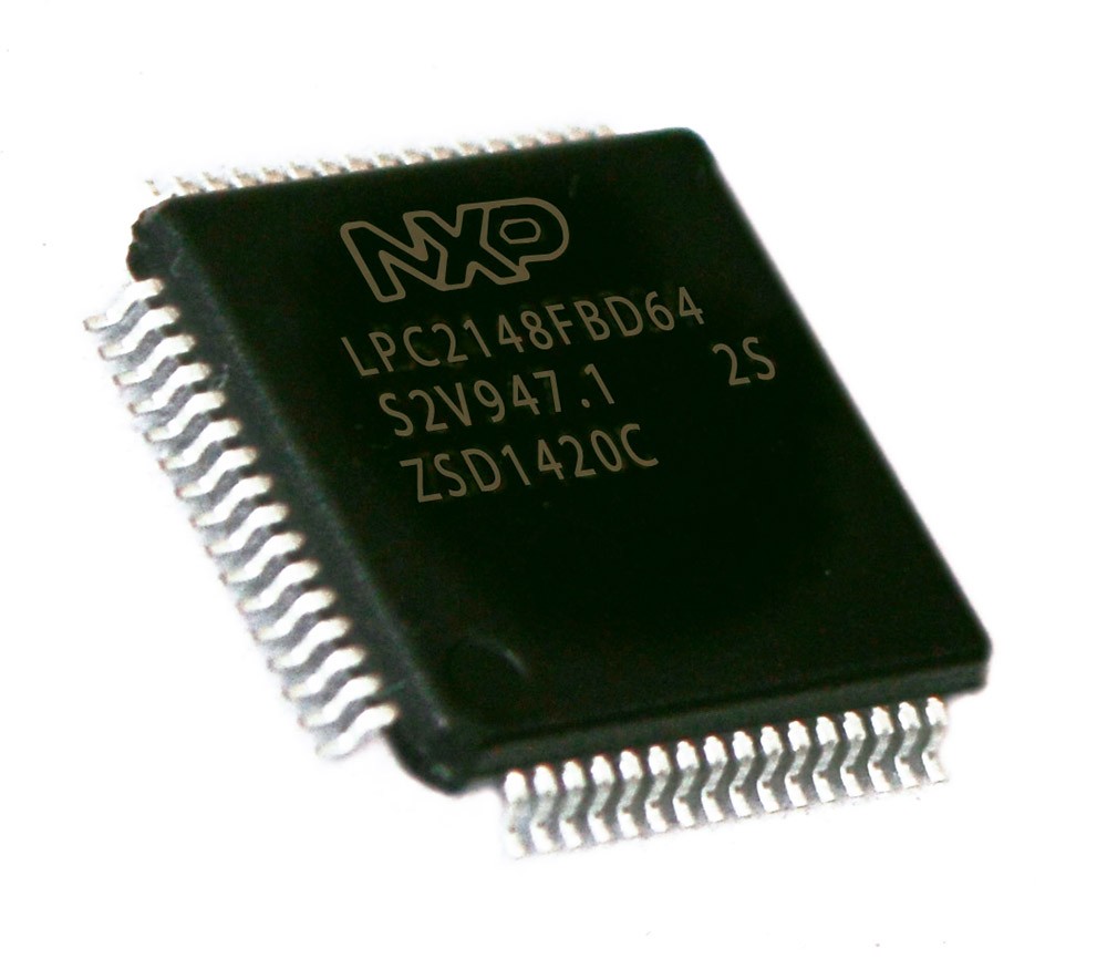
ARM7
Ficha técnica
Historia
ARM7 is a group of older 32-bit RISC ARM processor cores licensed by ARM Holdings for microcontroller use. The ARM7 core family consists of ARM700, ARM710, ARM7DI, ARM710a, ARM720T, ARM740T, ARM710T, ARM7TDMI, ARM7TDMI-S, ARM7EJ-S. The ARM7TDMI and ARM7TDMI-S were the most popular cores of the family. Since ARM7 cores were released from 1993 to 2001, they are no longer recommended for new IC designs; instead ARM Cortex-M or ARM Cortex-R cores are preferred. 1993 ARM700 1994 ARM710 1994 ARM7DI 1994 ARM7TDMI 1995 ARM710a 1997 ARM710T
ARM7
Ficha técnica
Historia
ARM7 is a group of older 32-bit RISC ARM processor cores licensed by ARM Holdings for microcontroller use. The ARM7 core family consists of ARM700, ARM710, ARM7DI, ARM710a, ARM720T, ARM740T, ARM710T, ARM7TDMI, ARM7TDMI-S, ARM7EJ-S. The ARM7TDMI and ARM7TDMI-S were the most popular cores of the family. Since ARM7 cores were released from 1993 to 2001, they are no longer recommended for new IC designs; instead ARM Cortex-M or ARM Cortex-R cores are preferred. 1993 ARM700 1994 ARM710 1994 ARM7DI 1994 ARM7TDMI 1995 ARM710a 1997 ARM710T
ARM7
Ficha técnica
Historia
ARM7 is a group of older 32-bit RISC ARM processor cores licensed by ARM Holdings for microcontroller use.
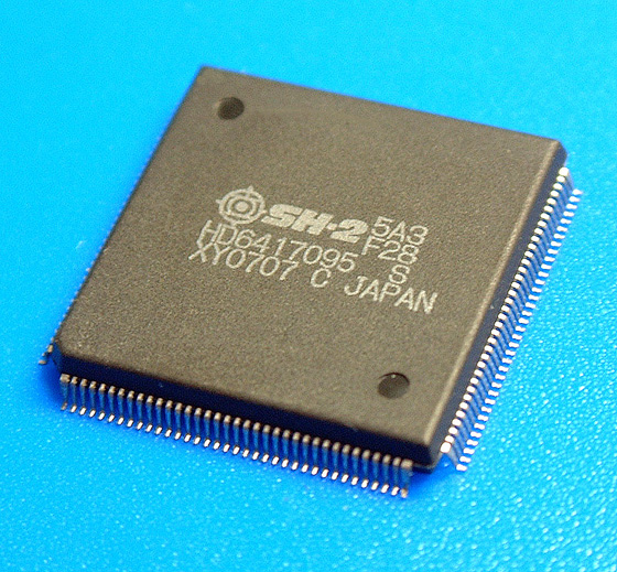
Hitachi SH-2
Ficha técnica
Historia
The SuperH processor core family was first developed by Hitachi in the early 1990s. Hitachi has developed a complete group of upward compatible instruction set CPU cores. The SH-1 and the SH-2 were used in the Sega Saturn, Sega 32X and Capcom CPS-3.[2] These cores have 16-bit instructions for better code density than 32-bit instructions, which was a great benefit at the time, due to the high cost of main memory.
Cyrix 486 DX
Ficha técnica
Historia
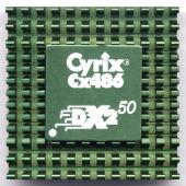
The Cyrix Cx486DX was designed to be completely software-compatible with Intels i486DX processor. It is not just an Intel clone but a completely new design by Cyrix. Compared to the i486DX the Cx486DX had an improved cache algorithm and therefore was faster in specific applications. The price for a Cx486DX was a little lower than for Intels 486DX and made the processor a very common i486DX alternative.
Intel DX4
Ficha técnica
Historia
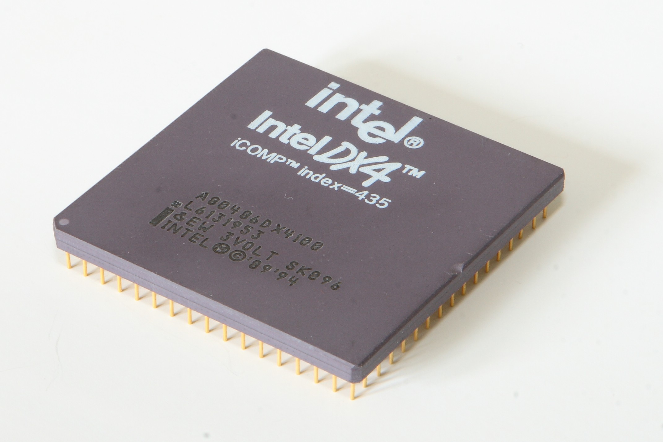
The IntelDX4 is a clock-tripled i486 microprocessor with 16 KB L1 cache. Intel named it DX4 (rather than DX3) as a consequence of litigation with AMD over trademarks. The product was officially named the IntelDX4, but OEMs continued using the i486 naming convention
Intel Pentium
Ficha técnica
Historia
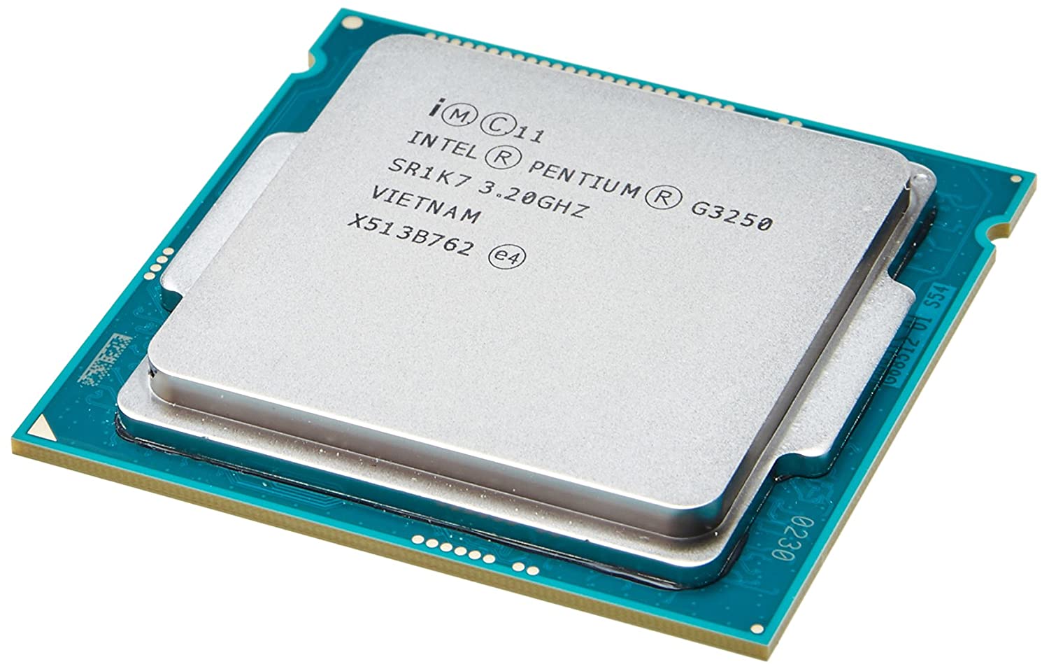
The successor to the 486. It has two 32-bit 486-type integer pipelines with dependency checking and can execute a maximum of two instructions per cycle. It does pipelined floating-point and performs branch prediction. It has 16 kilobytes of on-chip cache, a 64-bit memory interface, 8 32-bit general-purpose registers and 8 80-bit floating-point registers. Intel called its 586 processor Pentium because a US court ruled that you cant trademark a number.
AMD Am5x86
Ficha técnica
Historia
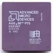
Introduced in November 1995, the AMD 5x86 is a standard 486 processor with an internally-set multiplier of 4, allowing it to run at 133 MHz on systems without official support for clock-multiplied DX2 or DX4 486 processors. Like most of the later 486 parts, the 5x86 featured write-back L1 cache, and unlike all but a few, a generous 16 kilobytes rather than the more common 8KB. Since having a clock multiplier of four was not part of the original Socket 3 design, AMD made the 5x86 look for a two times setting from the motherboard and interpret that as four times instead. In other words, to use the 5x86 you want to set the motherboard to the 2x setting. This will actually cause the 5x86 to run at 4x. The combination of best-in-class clock speed and the write-back cache allowed the 5x86 to equal or slightly surpass an Intel Pentium 75 MHz processor in business application performance. Also, because it was based on a pure 486 design, it was compatible with older systems, something its slightly faster rival, the Cyrix 5x86, had trouble with.
Cyrix 5x86
Ficha técnica
Historia
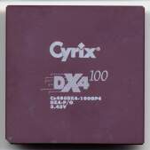
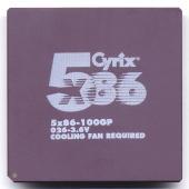
The 5x86 processor utilizes efficient fifth-generation (Pentium class) architectural features to significantly improve performance while minimizing transistor count. It achieves this performance using a superpipelined architecture in the integer unit combined with data forwarding, branch prediction, a 16-KByte unified write-back cache, single-cycle instruction decode, and single-cycle execution. The processors built-in power-saving features automatically power down the Floating Point Unit (FPU) and other idle internal circuits, while the System Management Mode (SMM) conserves power flowing to system peripherals. The Cyrix 5x86 processor is an example of Cyrixs strategy to design next-generation processor architectures that leverage existing designs. It is available in a 168-pin PGA or a 208-pin QFP package with standard 486 pinout. Though its installed in a P24D socket on a 486 motherboard, the motherboard must have a BIOS that will support the 5x86.
Cytrix 6x86
Ficha técnica
Historia
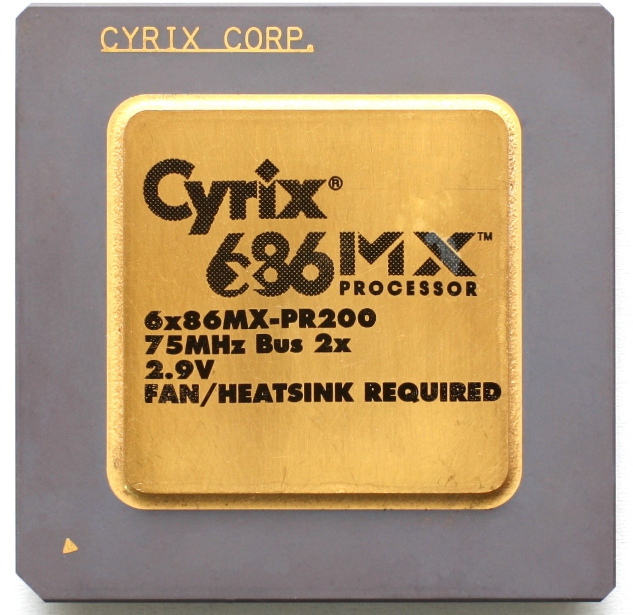
Cyrix entered the fifth generation processor market with the 6x86 processor, formerly projected as the M1. As a successful and cheaper (often less than half the cost) alternative to the Intel Pentium, it is pin- and voltage-compatible with it. Cyrix gave it the 6x86 name in reference to some of its more advanced features, which it calls sixth generation. In reality, the processor is comparable in power and architecture to the fifth-generation Pentium. The 6x86 is not a Pentium clone. Clones are exact or near-exact copies, usually being reversed engineered or based on licensed code. The 6x86 is based on an original Cyrix design. It incorporates several advanced architectural features that allow it to outperform a Pentium of equal clock speed. For this reason Cyrix helped invent the P-Rating system. This was an advantage to help people make a valid comparism but also caused some confusion when setting the appropriate clock speed on the motherboard. The Cyrix 6x86 range has the most powerful processor core of any x86 processor of its generation. Unfortunately, like the AMD K5, it also has a very slow floating point math capability and so was a very poor games and 3D performer. The processor is designed for Socket 7 and is available in several clock speeds, some of them rather unusual. The 6x86 PR200 (150 Mhz) processor introduced non-standard bus speeds up to 75 MHz - many motherboards and PCI cards did not support this speeds: Since the PCI bus runs at half of the mainboard bus speed, you are increasing the PCI bus to 37.5 MHz with a bus speed of 75 MHz. Several PCI cards, especially some graphics cards, did not run correctly with this overclocked bus.
IBM PowerPC 603
Ficha técnica
Historia
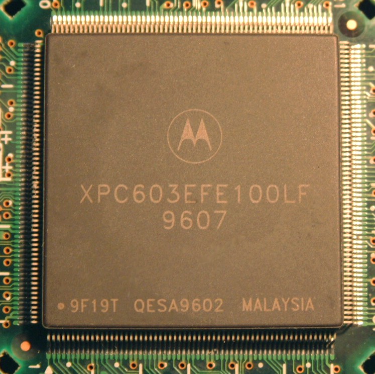
The PowerPC 600 family was the first family of PowerPC processors built. The first incarnation became the PowerPC 601 in 1993, and the second generation soon followed with the PowerPC 603, PowerPC 604 and the 64-bit PowerPC 620 The PowerPC 603 was the first processor implementing the complete 32-bit PowerPC Architecture as specified. It was designed to be a low cost, low end processor for portable and embedded use. One of the main features was power saving functions (doze, nap and sleep mode) that could dramatically reduce power requirements, drawing only 2 mW in sleep mode. The 603 has a four-stage pipeline and five execution units: integer unit, floating point unit, branch prediction unit, load/store unit and a system registry unit. It has separate 8 KB L1 caches for instructions and data and a 32/64 bit 60x memory bus, reaching up to 75 MHz. The 603 core did not have hardware support for SMP. A 200 MHz Motorola PowerPC 603 in a ceramic Ball Grid Array packaging. The PowerPC 603 had 1.6 million transistors and was fabricated by IBM and Motorola in a 0.5 μm CMOS process with four levels of interconnect. The die was 85 mm2 large drawing 3 W at 80 MHz. The 603 architecture is the direct ancestor to the PowerPC 750 architecture, marketed by Apple as the PowerPC G3. The 603 was intended to be used for portable Apple Macintosh computers but could not run 68K emulation software with performance Apple considered adequate, due to the smaller processor caches. As a result, Apple chose to only use the 603 in its low-cost desktop Performa line
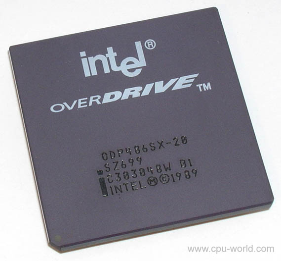
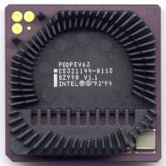
Intel Pentium Overdrive For 486
Ficha técnica
Historia
This Pentium OverDrives are Intel Pentium processors for 486 Socket 3 and Socket 2 motherboards, provided as a means to give a Pentium performance-level upgrade option for owners of 486 computer systems. It was however criticised for being more expensive and slower than competing CPU-upgrade options such as the AMD Am5x86 and Cyrix 5x86, and being too late to the market. Mainboard compatibility was also a problem, it turned out that many boards didnt support this new chip. To perform properly, the Pentium OverDrive was dependent on a high amount of secondary cache ram being present on the motherboard; without it the chip was only a trivial amount faster than a DX4.
Página 2 de 4