Inicio › Ordenadores › Microprocessors

Microprocessors

💾 Ordenadores182 fichaspágina 3/4

Máquinas (121–180 de 182)

Intel Pentium Pro
Intel Pentium Pro
📅 1995
Ficha técnica

Historia

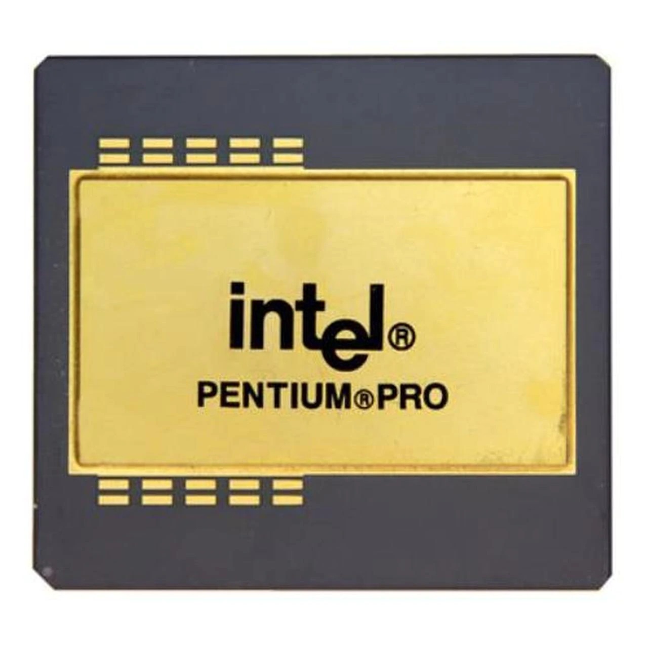
The Pentium Pro is a sixth-generation x86 architecture microprocessor by Intel originally intended to replace the original Pentium in a full range of applications, but later reduced to a more narrow role as a server and high-end desktop chip. It was introduced using an enormous rectangular Socket 8 form factor in November 1995. Intel has since discontinued it in favor of the newer high-end Xeon processor lines. Despite the name, the Pentium Pro is actually quite different from Intels earlier Pentium processor, being based on the then-new P6 core (which in a modified form would later be used for the Pentium II, Pentium III and Pentium M). The P6 core features out-of-order execution, speculative execution, and an additional pipe for simple instructions. Intel called its 586 processor Pentium because a US court ruled that you cant trademark a number.
Motorola 68040
Motorola 68040
📅 1995
Ficha técnica

Historia

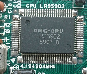
Nintendo Game Boy, based on Z80

Nec VR4300
Nec VR4300
📅 1995
Ficha técnica

Historia

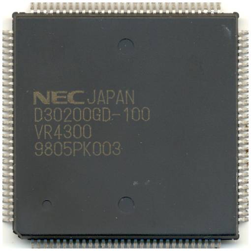
The Nintendo 64s central processing unit (CPU) is the NEC VR4300,a cost-reduced derivative of the 64-bit MIPS Technologies R4300i.

SunPlus SPG280
SunPlus SPG280
📅 1995
Ficha técnica

Historia

There is one Chinese company with several names that makes chips that you could probably find in devices you already own: SunPlus. The SPG2xx series use a custom instruction set (“u’nSP”), and are designed for something like the TV Plug-n-Play games; they are used in most (if not all) of those, as well as the Vii and the V.smile (if nothing else). Segher took our dumped ROM and scant documentation and built a disassembler, and then a mostly-working emulator for this architecture (more on this below). The top of the line SPG290 uses a different “s+core” architecture, and is used in the Mattel Hyperscan. Jakks Pacific TV Plug’n’Play games also use SPG chips SPMP The SPMP series chips are ARM-based SoCs that are used in cheap Chinese “Personal Media Players” that also generally come bundled with NES or GameBoy emulators.

AMD 5k86
AMD 5k86
📅 1996
Ficha técnica

Historia

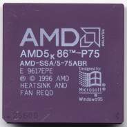
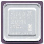
The 5k86 is AMDs 5th generation x86 implementation, introduced in March 1996. The processor, later renamed to K5, was eagerly awaited and it was hoped that it would provide a viable alternative to the Pentium early in the Pentiums life cycle. Unfortunately, AMD delivered the processor over a year late and at much lower clock speeds than had been originally anticipated. As a result instead of being the Pentium killer AMD had hoped for, the K5 was positioned as a low-cost Pentium alternative. The K5 is, internally, a very advanced processor, the most advanced of the fifth-generation chips. Internally it is more comparable to the Pentium Pro. It is an x86 translation/emulation processor, decoding x86 instructions into RISC-like microinstructions and executing them on a 6-pipeline internal core. This allows the K5 to achieve higher performance than a Pentium of the same speed.

AMD K5
AMD K5
📅 1996
Ficha técnica

Historia

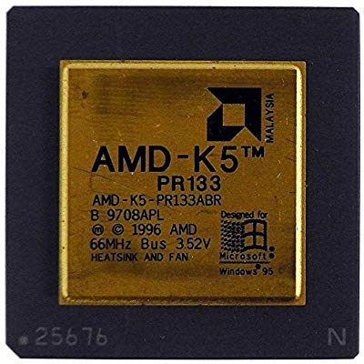
The K5 was developed by AMD to compete with Intels Pentium microprocessor range. Introduced in 1996 almost 2 years late, AMDs problems were compounded by being unable to manufacture the chip at the clock speeds originally projected. In its favor, the K5 did at least offer good x86 compatibility. All models had 4.3 million transistors on-chip. No K5 supported MMX instructions. Internally ambitious, it was closer to a Pentium Pro than a Pentium, based upon an internal highly parallel RISC processor architecture with an x86 decoding front-end. Improvements and differences to the Intel Pentium include: Five integer units, which could process instructions out of order, one floating point unit, compared to two units of the Pentium The branch target buffer was four times the size of the Pentiums, although not reportedly more accurate Register renaming improved parallel performance of the pipelines Speculative execution of instructions reduced pipeline stall The instruction cache is 16 Kb, double the Pentium The primary cache is 4-way set associative instead of the Pentiums 2-way The K5 project represented an early chance for AMD to take technical leadership from Intel. Although the chip addressed the right design concepts, the actual engineering implementation was weak. The low clock rates were due in part to AMDs deficiencies as a manufacturing company in the period. However, having a branch prediction unit four times the size of the Pentium, yet reportedly not delivering superior performance, is an example of how the actual implementation fell short of the project goals. Additionally, while the K5s floating point performance was better than that of the Cyrix 6x86, it was weaker than that of the Pentium. Because it was late to market and did not meet performance expectations, the K5 never gained the acceptance among large computer manufacturers that the Am486 and AMD K6 enjoyed. Overall, the chip failed to deliver, both in terms of raw performance, and financially for AMD.

Cyrix Media GX
Cyrix Media GX
📅 1996
Ficha técnica

Historia

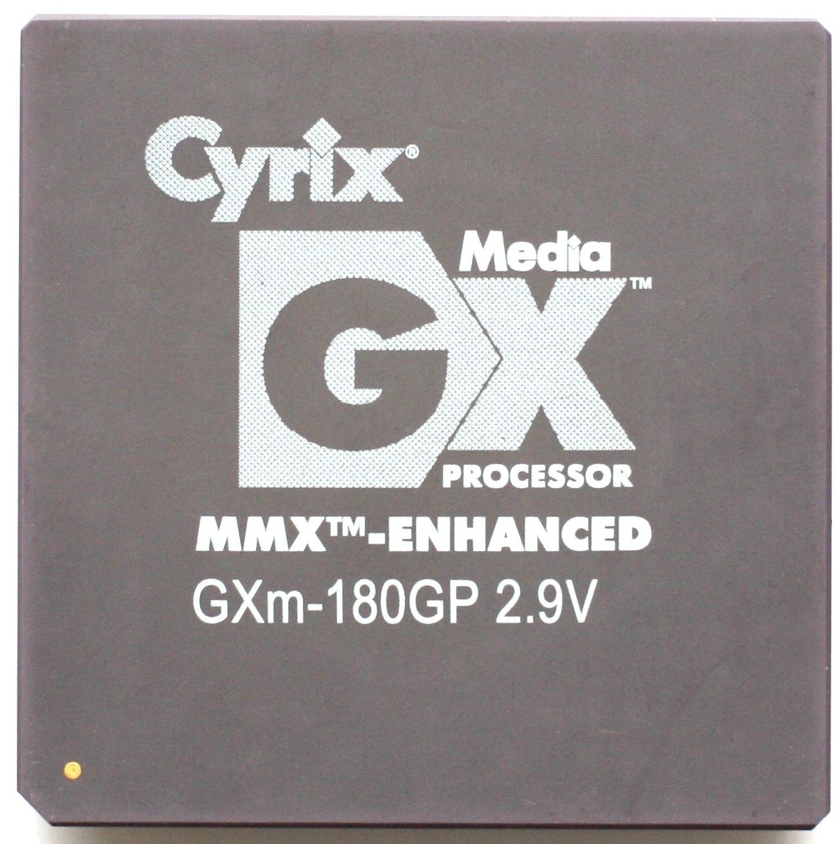
In 1996 Cyrix released the MediaGX CPU, which integrated all of the major discrete components of a PC, including memory controller, graphics, sound and PCI controller, onto a single chip. Initially based on the old 5x86 technology and running at 120 or 133 MHz, its performance was widely criticized but its low price made it quite successful. Though it required a special motherboard and was not pin compatible with the Pentium, it was the cheapest route into a Pentium class system available on the market. Later versions of the MediaGX ran at speeds of up to 333 MHz and added MMX support. A second chip was added to extend its video capabilities. The MediaGX led to Cyrixs first big win, when Compaq used it in its lowest-priced Presario computers. This led to further MediaGX sales to Packard Bell and also seemed to give Cyrix legitimacy, as 6x86 sales to Packard Bell and eMachines quickly followed. But because it seemed to have so much potential in the low-cost market, it dragged Cyrixs attention away from the main market - high-performance desktop parts - and attracted the interest of other companies, notably National Semiconductor, which bought Cyrix in July 1997 largely on the strength of the MediaGX design, and over the next year or so proceeded to mismanage the company into oblivion.

Intel Pentium MMX
Intel Pentium MMX
📅 1996
Ficha técnica

Historia

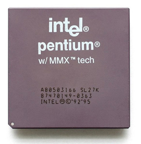
In October 1996 Intel released the 4th Pentium generation as the Pentium with MMX Technology (usually just called Pentium MMX); it was based on the standard Pentium core, the 0.35 �m process of 3rd generation Pentiums was also used for this series, but it had a new set of 57 MMX (MultiMedia eXtensions) instructions to improve working on multimedia tasks, such as encoding and decoding media. However, software must be specially optimized to make use of MMX, and the increased speed the Pentium MMX showed at its apparition was mainly due to the fact that the internal cache had been doubled in size to 32 KB.

AMD K6
AMD K6
📅 1997
Ficha técnica

Historia

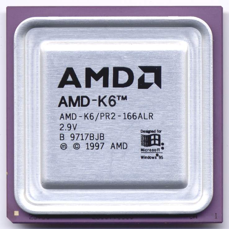
After AMDs plans with the K5 turned into a debacle, AMD again claimed that they had the solution to make them more than just discount alternatives to Intel: A chip with the power of a Pentium Pro, with MMX support and intended to fit into a standard socket 7. AMD delivered its much anticipated K6 chip in April of 1997, beating Intels Pentium II to the market by a month. AMD showed their commitment to establishing themselves in the market when they purchased NexGen in 1996 and with it, the design for the Nx686 processor. NexGen had been intending to market this chip in its own socket, but AMD changed the design to fit the standard socket 7, added MMX support, and renamed it the K6. Despite the name implying a design evolving from the K5, it is in fact a totally different design that was created by the NexGen team and adapted after the AMD purchase. The K6 was originally launched running at speeds of 166 and 200 MHz in April 1997. It was followed by a 233 MHz version later in the summer of 1997. The release of the 266 MHz version of this chip was not until spring 1998 when AMD were able to move to the 0.25 micron manufacturing process. The final iteration of the K6 design was released in May 1998 running at 300 MHz and continued with the K6-2. Initially, the AMD K6 processors used Pentium II Rating (PR2) to designate their speed. The PR2 rating was dropped because the rated frequency of the processor was the same as the real frequency. This item was made in the month the K6 was released (week 17/1997 = April 21st - 27th, 1997) and has the initial PR2 marking.

Cyrix 6x86 MX
Cyrix 6x86 MX
📅 1997
Ficha técnica

Historia

The successor to the 6x86 and 6x86L is the 6x86MX (M2), introduced May 30, 1997 and intended to compete with AMDs K6 and Intels Pentium MMX. The 6x86MX is an evolutionary step from the 6x86 and is very similar to it in internal function. The 6x86MX supports the MMX extension and also features several other improvements over the original 6x86 chip. The internal cache was increased from 16 to 64 KB, a 256 byte additional pre-cache was added to help improve efficiency in how the regular level 1 cache is operated, the Branch Prediction was improved and the internals of the chip have been optimized for 32-bit operation.

Intel Pentium II
Intel Pentium II
📅 1997
Ficha técnica

Historia

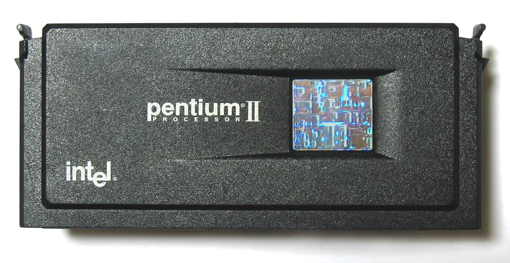
The Pentium II is a sixth-generation x86 architecture microprocessor by Intel, introduced on May 7, 1997. It was based on a modifed version of the P6 core first used for the Pentium Pro, but with improved 16-bit performance and the addition of the MMX instructions which had already been introduced on the Pentium MMX. Unlike previous Intel processors such as the Pentium and Pentium Pro, the Pentium II was packaged in a slot-based form-factor rather than a socket one. This larger package was a compromise allowing Intel to separate the secondary cache from the processor while still keeping it on a closely coupled bus. This separate cache was slower (running at half the processor speed) than that in the Pentium Pro, but solved the Pentium Pros low yields allowing Intel to introduce the Pentium II at a mainstream price level. A low-end version of the Pentium II - essentially a Pentium II with less (or no) level 2 cache - was marketed under the name Celeron. The Pentium II Xeon was a high-end version intended for use on servers. By early 1999, the Pentium III superseded the Pentium II.

Intel Pentium MMX Overdrive
📅 1997
Ficha técnica

Historia

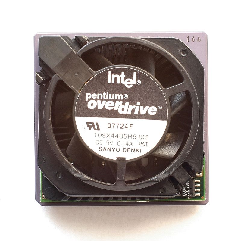
With the introduction of the Intel Pentium with MMX Technology, Intel also created OverDrive processors to upgrade existing Pentium motherboards to the new MMX chip. Most older Pentium motherboards cannot handle the new Pentium with MMX because of its requirement for a 2.8V core. Keeping with the tradition of Intels OverDrive line, the Pentium with MMX OverDrive includes a converter that lets it run in Socket 5 motherboards (except for the 200) and Socket 7s that do not have 2.8V support. Otherwise the chip is identical to the standard Pentium with MMX.

Motorola MC68HC05
Motorola MC68HC05
📅 1997
Ficha técnica

Historia

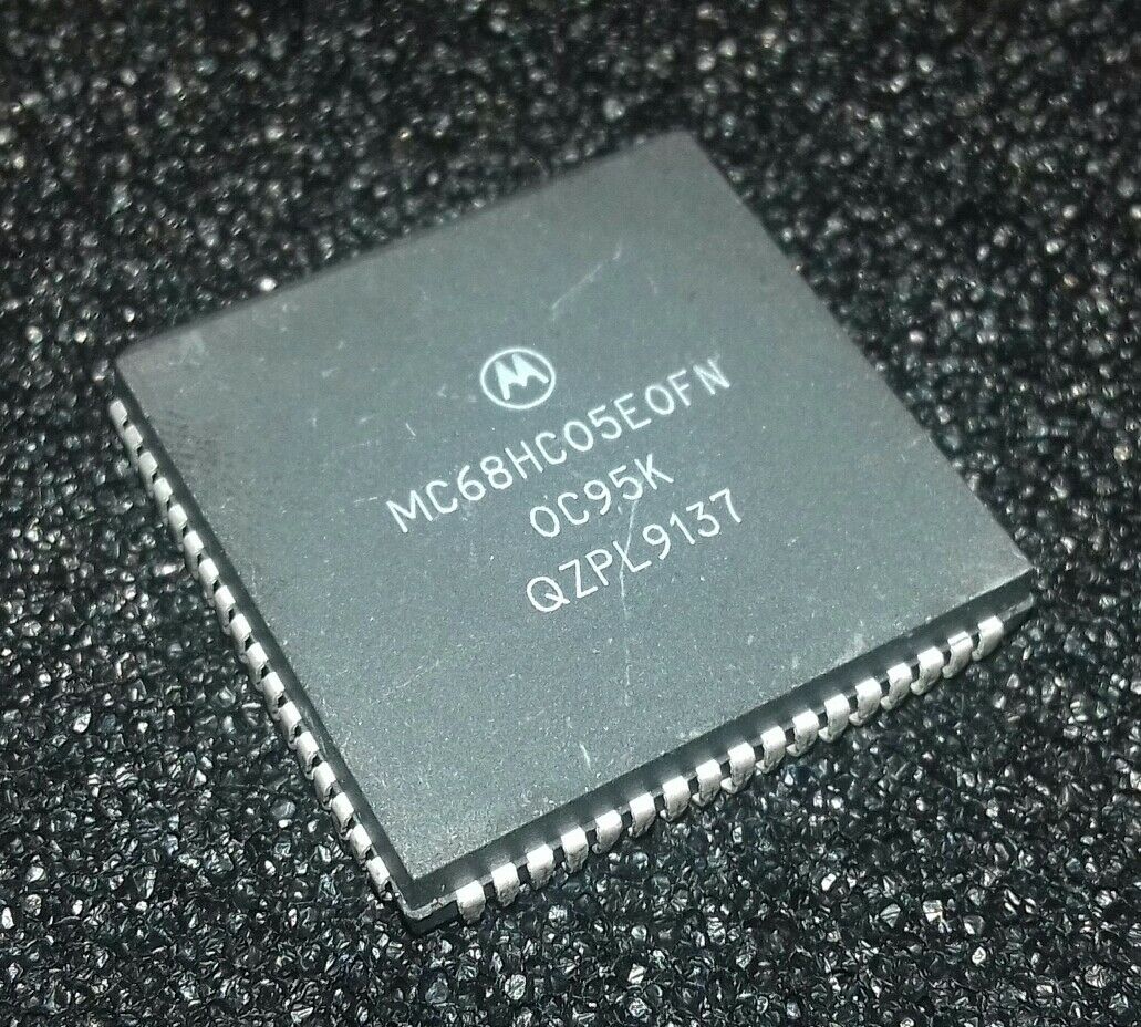
The 68HC05 (HC05 in short) is a broad family of 8-bit microcontrollers from Freescale Semiconductor (formerly Motorola Semiconductor). Like all Motorola processors that share lineage from the 6800, they use the von Neumann architecture as well as memory-mapped I/O. This family has five CPU registers that are not part of the memory: an 8-bit accumulator A, an 8-bit index register X, an 8-bit stack pointer SP with two most significant bits hardwired to 1, a 13-bit program counter PC, and an 8-bit condition code register CCR. Among the HC05s there are several processor families, each targeted to different embedded applications. The 68HC05 family broke ground with the introduction of the EEPROM-based MC68HC805C4 and MC68HC805B6 variants in the late 1980s. Using a serial bootloader, they could be programmed in-circuit with simple software running on a PC and a low current 19V supply (no programmer required).

Motorola PowerPC 604
📅 1997
Ficha técnica

Historia

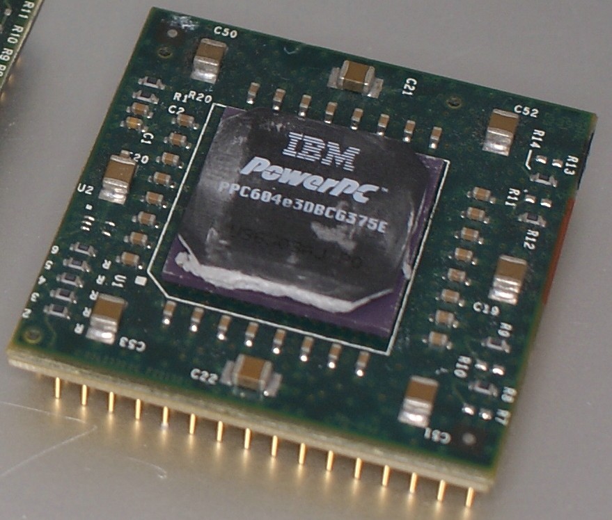
The PowerPC 604 was the high end PowerPC when released, performing at 1.5 times the speed of a PowerPC 601 at equal clock speeds. The chip was later updated by doubling the L1 cache to 64KB and shrinking the processor, now dubbed the 604e. The fastest versions of the 604e version were nicknamed Mach 5 and ran at 250-350MHz.

AMD K6-2
AMD K6-2
📅 1998
Ficha técnica

Historia

The K6-2 was a significant improvement over the K6. It built upon the K6s processing core, with the addition of 21 new instructions called 3D Now!. These are SIMD (Single Instruction Multiple Data) instructions designed to enhance the 3D geometry capability of the chips floating point unit. This allowed the K6-2 to overcome the handicap of the slow (relative to Intel) CPU which the K6 owned. The K6-2 also saw the introduction of a 100 MHz front side bus. This was only available to owners of new Super Socket 7 motherboards which also included features such as AGP. All of these features helped to give the K6-2 performance fast enough to be a credible challenger to the dominant Pentium II. Performance of the two chips was broadly similar: the K6-2 tending to be faster for general-purpose computing, the Intel part clearly superior at floating-point tasks. The K6-2 was a very successful chip and provided AMD with the marketing base and the financial stability it would need to introduce the Athlon. The K6-2 was originally manufactured in speeds of 266 & 300 MHz in May 1998. The 300 MHz chip saw the introduction of the 100 MHz bus over the conventional 66 MHz bus used by the 266 MHz chip. August 1998 a 333 MHz version on a 95 MHz bus has been released and was quickly followed by a 350 MHz version on the 100 MHz bus. November 1998 saw the release of the 366, 380 and 400 MHz versions of the chip. This has been followed by the release of a 450 MHz K6-2 in February 1999 and the 500 MHz version in August 1999.

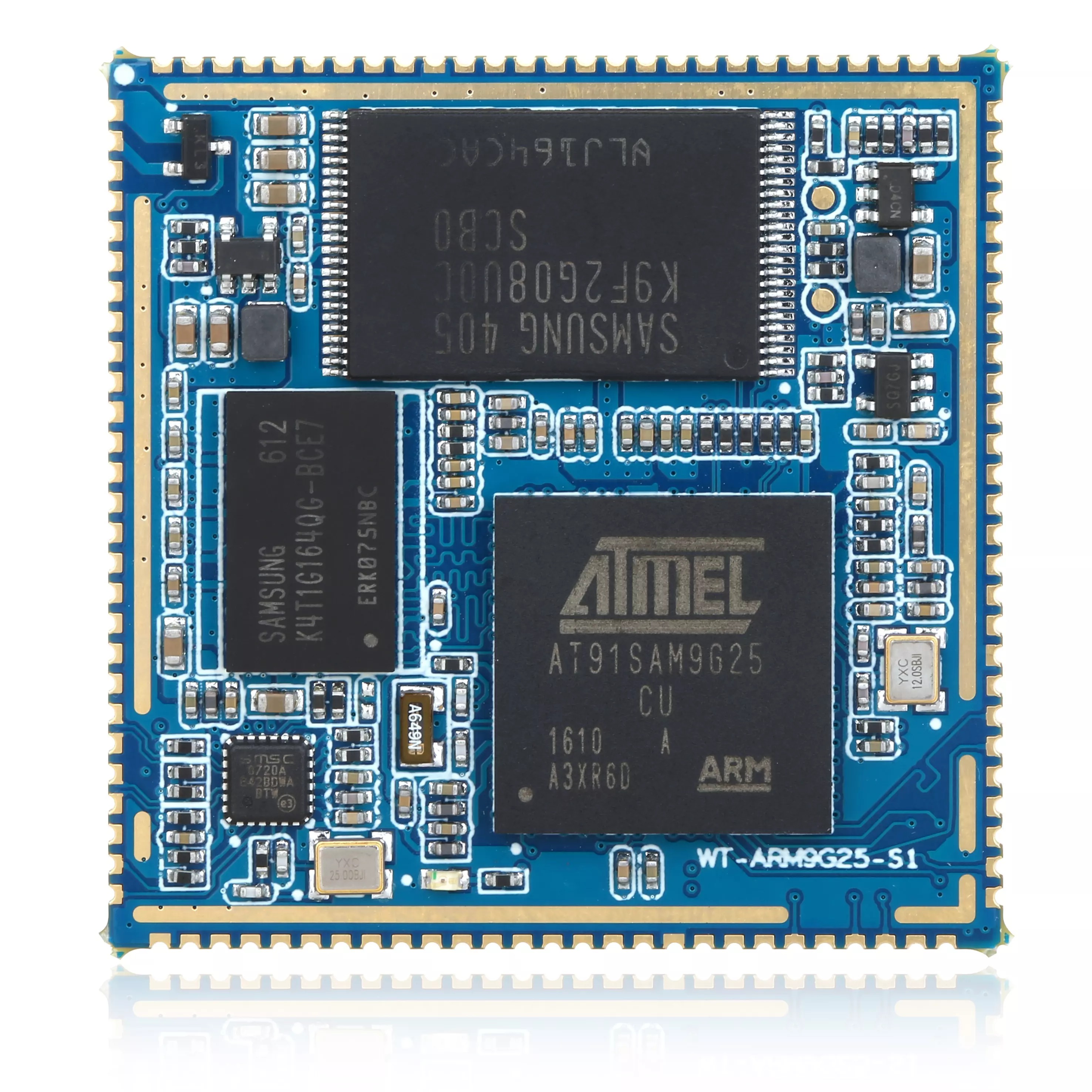
ARM9
ARM9
📅 1998
Ficha técnica

Historia

ARM9 is a group of older 32-bit RISC ARM processor cores licensed by ARM Holdings for microcontroller use. The ARM9 core family consists of ARM9TDMI, ARM940T, ARM9E-S, ARM966E-S, ARM920T, ARM922T, ARM946E-S, ARM9EJ-S, ARM926EJ-S, ARM968E-S, ARM996HS. Since ARM9 cores were released from 1998 to 2006, they are no longer recommended for new IC designs, instead ARM Cortex-A, ARM Cortex-M, ARM Cortex-R cores are preferred.

ARM9
ARM9
📅 1998
Ficha técnica

Historia

ARM9 is a group of older 32-bit RISC ARM processor cores licensed by ARM Holdings for microcontroller use.

Cyrix MII
Cyrix MII
📅 1998
Ficha técnica

Historia

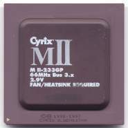
After Cyrix was purchased by National Semiconductor in 1997 they terminated their foundry agreement with IBM. National fabricated their own chips and the 6x86MX was re-named MII. Compared to early 6x86MX CPUs the MII had some enhancements to its processor core. Heat output was reduced allowing it to rise to clock speeds over 220MHz. The MII also required non-standard bus speeds at 75 or 83MHz on socket 7 boards and therefore had some troubles with stability.

Intel Pentium II Celeron
📅 1998
Ficha técnica

Historia

The Celeron family is a line of budget x86 processors based on Pentium P6 designs. It is marketed by Intel as a second line to complement their more expensive but higher-performance Pentium CPUs. The first Celeron was introduced in April 1998 and based on the Pentium II. Later versions are based on the Pentium III and Pentium 4 designs. The Celeron product concept was introduced by Intel in response to the companys loss of low-end market share, in particular to Cyrixs 6x86 and AMDs K6, but also to other competers such as the IDT Winchip. Intels venerable Pentium MMX was no longer performance competitive and although a faster Pentium MMX would be cheap to make and technically straightforward, Intel preferred to move away from the industry standard Socket 7 platform (for which competitors made drop-in replacement CPUs) and produced a budget part that was pin-compatible with their high-end Pentium II product (Slot 1). For both technical and legal reasons, competitors had difficulty making Slot 1 parts.

Intel Pentium II Xeon
📅 1998
Ficha técnica

Historia

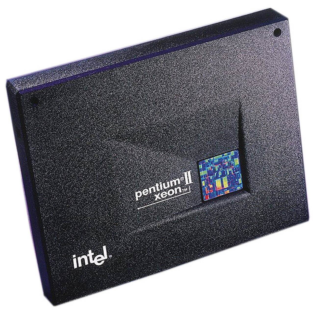
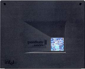
The Pentium II Xeon was introduced in June 1998 as Intels new line of server and workstation processors. The PII Xeon core, manufactured in a .25 micron process, is not much different from the Pentium IIs core. It added multiprocessing support for quad CPU systems and even 8 CPUs in one system and a few enhancements, such as support for more than 4GB of memory. The biggest difference in both performance and architecture comes from the PII Xeon’s L2-cache, at 512KB, 1 or even 2 MB and running at full clockspeed, while the Pentium II was only offered with a 512KB L2 cache running at half CPU clockspeed. The PII Xeon also introduced Intels biggest processor module so far (about twice the size of a Pentium II cartridge) to include the CPU core and up to four 512KB L2 cache chips.

Motorola PowerPC 740 750
📅 1998
Ficha técnica

Historia

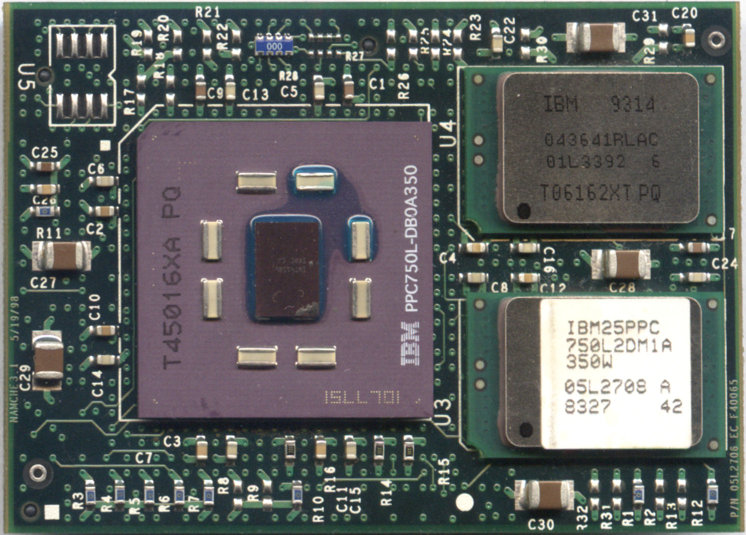
Codenamed Arthur, the PowerPC G3 name comes from the third generation of PowerPC microprocessor. It was used in Apple Macintosh computers such as the PowerBook G3, the iMacs, iBooks and several desktops, including the Power Macintosh G3s. The G3 was introduced in two different versions, derived from the PPC 603 series of microprocessors: the PPC 740 and PPC 750 microprocessors. The PPC 740 slightly outperformed Pentium IIs while consuming less than 20% of the amount of power and size. Derived from the PPC 740, the PPC 750 had a faster way to access L2 cache, which allowed higher performance. The earlier versions, made by Motorola, used an aluminium process for fabrication, and were limited to 400 MHz speeds. Later versions, manufactured by IBM with a silicon-on-insulator fabrication process, achieved speeds of 500 MHz and beyond. All G3 versions did not completely implement a standard for symmetric multiprocessing computers, which made design and manufacture of a SMP computer comparatively difficult. The PowerPC G4 corrected this deficiency. With its combination of small size and low power requirements, the G3 proved an ideal laptop microprocessor in its era. Apple ceased using the G3 on October 22, 2003.

Motorola PowerPC 7400
📅 1998
Ficha técnica

Historia

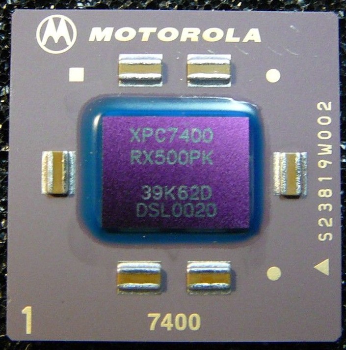
The fourth generation of PowerPC processors, the PPC G4, is used in Apple Macintosh computers such as the G4 PowerBook, the 2nd generation Flat Panel iMac, the eMac, the 3rd generation iBook, and the desktop G4 Power Mac. Most of the G4 design was done by Motorola in close cooperation with Apple. IBM, the third member of the AIM alliance, chose not to participate in the design of the G4 in part owing to microprocessor design disagreements concerning a Vector Processing Unit on the chip. Ultimately, the G4 architecture design contained a 128-bit vector processing unit called AltiVec. With the AltiVec unit, the G4 microprocessor can do four-way single precision floating point math, or 16-way byte math in a single cycle. Furthermore, the vector processing unit on the G4 is superscalar, and can do two vector operations at the same time. Compared to Intels x86 microprocessors at the time, this feature offered a substantial performance boost, if the application was coded to take advantage of the AltiVec unit.

AMD Athlon
AMD Athlon
📅 1999
Ficha técnica

Historia

The Athlon made its debut on August 21, 1999. The original Athlon core revision, codenamed K7, was available in speeds of 500 to 650 MHz at its introduction and was later sold at speeds up to 1000 MHz. Internally, the Athlon was essentially a major reworking of the K6 processor core designed for compatibility with the EV6 bus protocol (first used on DECs Alpha 21264 RISC processor). AMD dramatically improved the floating-point unit from the K6 and put a large 128K level 1 cache on the chip. Like on the Intel Pentium II there was 512k of secondary cache, mounted on the CPU module and running at a lower speed than the core. The resulting processor was the fastest x86 in the world. Various different versions of the Athlon held this distinction continuously from August 1999 until January 2002.

AMD K6-III
AMD K6-III
📅 1999
Ficha técnica

Historia

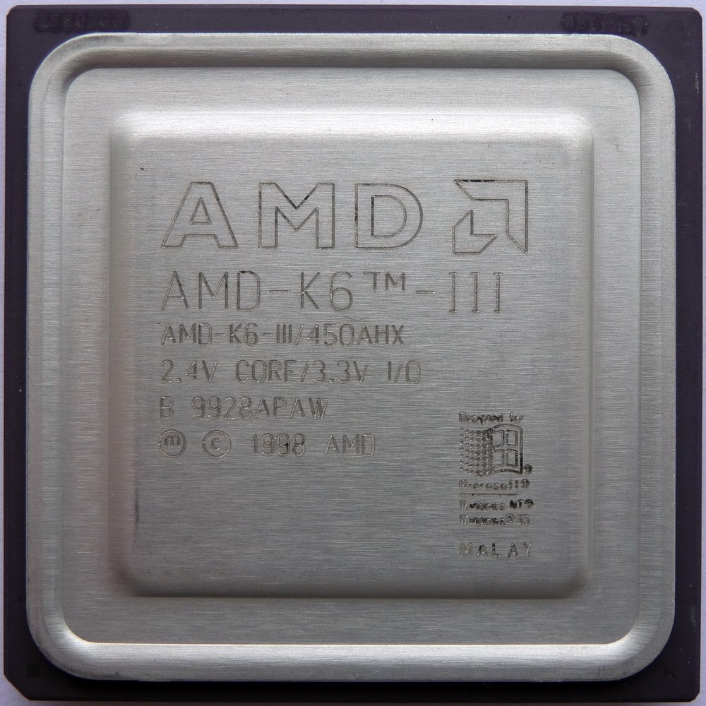
The K6-III was the last and fastest of all Socket 7 processors. It achieved the distinction of being the fastest x86 processor on the market on release, and remained highly competitive for a considerable time afterwards. In conception, the design was simple: it was a K6-2 with an additional L2 cache. The original K6-2 had a 64 KB primary cache and a much larger amount of motherboard-mounted cache (usually 512 KB or 1 MB but varying depending on the choice of main board). In contrast the competing Intel parts used 32 KB of L1 cache and either 128 KB of full-speed secondary cache integrated into the CPU itself (Celeron) or 512 KB of half-speed cache mounted on a processor daughter board (Pentium II, Pentium III). The K6-III, however, used both methods: it had 64 KB primary cache, a massive 256 KB on-chip, full-speed secondary cache (similar to the Celerons but twice the size), and the variable size motherboard mounted cache on the Socket 7 main board became a tertiary level. In execution, however, the design was not simple: with 21.4 million transistors, it was a very large chip to manufacture with early 1999 technology, and the K6 core design did not scale well past 500 MHz. Nevertheless, the K6-III 400 sold well, and the K6-III 450 was clearly the fastest x86 chip on the market on introduction, comfortably outperforming AMDs K6-2s and Intels Pentium IIs.

Hitachi SH-4
Hitachi SH-4
📅 1999
Ficha técnica

Historia

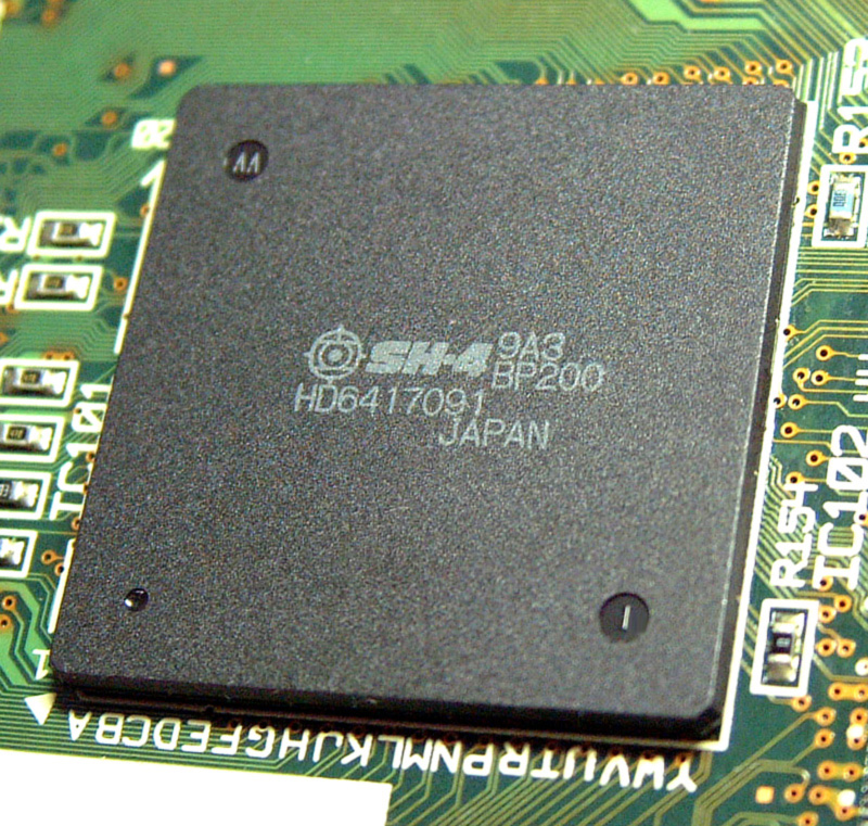
The SH-4 is a 32-bit RISC CPU and was developed for primary use in multimedia applications, such as Segas Dreamcast and NAOMI game systems. It includes a much more powerful floating point unit[note] and additional built-in functions, along with the standard 32-bit integer processing and 16-bit instruction size. SH-4 features include: FPU with four floating point multipliers, supporting 32-bit single precision and 64-bit double precision floats 4D floating point dot-product operation 128-bit floating point bus allowing 3.2 GB/sec transfer rate from the data cache 64-bit external data bus with 32-bit memory addressing, allowing a maximum of 4 GB addressable memory with a transfer rate of 800 MB/sec Built-in interrupt, DMA, and power management controllers

Intel Pentium II Overdrive
📅 1999
Ficha técnica

Historia

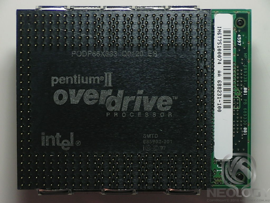
The Pentium II OverDrive is a processor upgrade designed for Pentium Pro (Socket 8) based systems. By using the 0.25 micron Deschutes core of the Pentium II, Intel managed to put a quick end to the 16-bit weakness of the Pentium Pro, and in doing so, they also managed to double the amount of L1 cache on the processor to 32KB. The PII OverDrive is nothing more than a Pentium II Xeon on a smaller scale, using the Pentium IIs design to place the L2 cache externally off of the CPU, but on a card that would allow it to operate at the same clock speed as the CPU itself. The chip has a built in clock multiplier of 5.0x, and it derives its clock speed based on the motherboards set FSB frequency, so on a 60Mhz board (150/180MHz Pentium Pro systems) the processor operates at 300MHz, on 66MHz systems (166/200MHz Pentium Pro) at 333MHz.

Intel Pentium III
Intel Pentium III
📅 1999
Ficha técnica

Historia

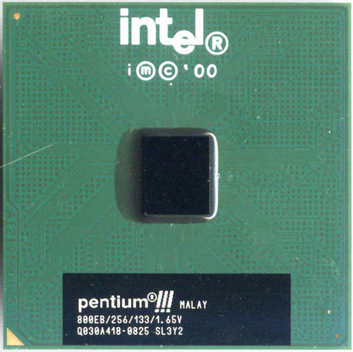
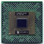
The Pentium III is an x86 (more precisely, an i686) architecture microprocessor by Intel, introduced on February 26, 1999. Initial versions were very similar to the earlier Pentium II, the most notable difference being the addition of SSE instructions. As with the Pentium II, there was also a low-end Celeron version and a high-end Xeon version. The Pentium III was eventually superseded by the Pentium 4. An improvement on the Pentium III design is the Pentium M.

Intel Pentium III Coppermine
📅 1999
Ficha técnica

Historia

The second Pentium III version, Coppermine, had an integrated full-speed 256 KB L2 cache with lower latency, which improved performance over Katmai. Under competitive pressure from AMDs Athlon processor, Intel also re-worked the chip internally, and finally fixed the well known instruction pipeline stalls. The result was a remarkable 30% increase in instruction processing performance. It was built on a 0.18 m process. Pentium III Coppermines running at 500, 533, 550, 600, 650, 667, 700, and 733 MHz were first released on October 25, 1999. From December 1999 to May 2000, Intel released Pentium IIIs running at speeds of 750, 800, 850, 866, 900, 933 and 1000 MHz (1GHz). A 1.13GHz version was released in mid-2000, but famously recalled after a popular hardware review website proved it was not stable enough to compile the Linux kernel. The problem was traced to the integrated cache, which simply could not operate at speeds above 1GHz. Intel needed at least six months to resolve this problem and released 1.1 and 1.13 GHz versions in 2001.

Intel Pentium III Xeon
📅 1999
Ficha técnica

Historia

The Pentium III Xeon was introduced in March 1999. Early versions (Code named Tanner) where built in .25 micron technology and featured a 100MHz front side bus, 512KB to 2MB L2 off-die cache sizes and multiprocessor support for up to 8 CPUs. In October 1999 Intel introduced the 2nd generation PIII Xeon Cascades, using the same core as the .18 micron Pentium III Coppermine processor. As a result the Cascades has its 256KB on-die L2 cache running at full clock speed and all the other Coppermine features like Advanced Transfer Cache, Advanced System Buffering, support for 133 MHz front speed bus, SSE (Streaming SIMD Extensions), etc. However, the introduction of Cascades had some severe drawbacks: The small 256KB L2 cache took back the Xeons performance advance over the standard Pentium III and the 133MHz bus protocol did not support more than 2 CPUs in a system. In May 2000 Intel finally released a large cache version with up to 2MB (on-die) L2 cache and 100MHz front side bus, again supporting multiprocessing with up to 8 CPUs.

Motorola PowerPC 860
📅 1999
Ficha técnica

Historia

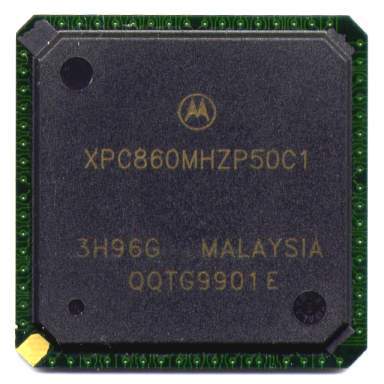
PowerQUICC Integrated Communications Processor The MPC860 PowerQUICC is a versatile one-chip integrated microprocessor and peripheral combination that can be used in a variety of controller applications, excelling particularly in communications and networking products.

Sony Emotion Engine
Sony Emotion Engine
📅 1999
Ficha técnica

Historia

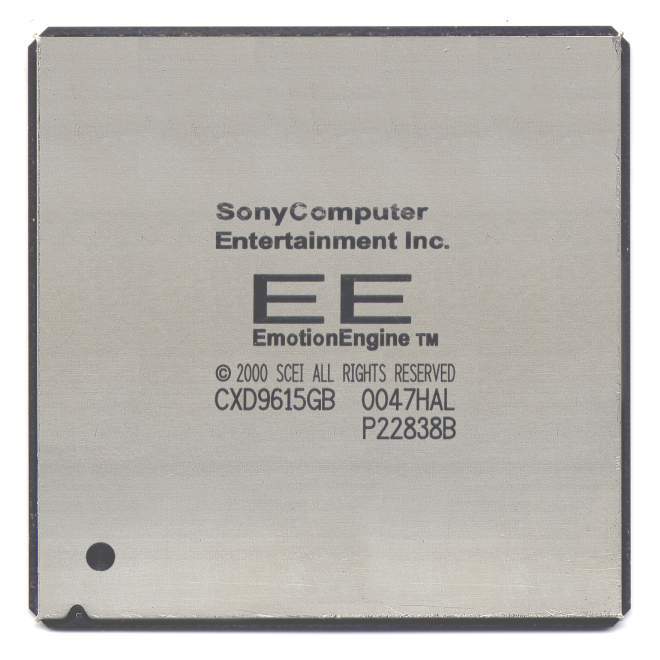
The Emotion Engine is the CPU for Sonys PlayStation 2, developed in a Sony - Toshiba cooperation and introduced in 1999. Data bus, cache memory as well as all registers are implemented in 128 bit technology, integrated on a single 0.18 micron process technology chip, making it the first commercial 128 bit CPU. The Emotion Engine, based on the MIPS R5900, is sort of a combination CPU and DSP processor, whose main function is simulating 3D worlds. It integrated all necessary units on the die: The MIPS III CPU core, 2 vector units, FPU, image processing unit (basically an MPEG2 decoder with some other capabilities), 10-channel DMA controller, graphics interface unit, RDRAM and I/O interfaces, all connected via a shared 128-bit internal bus.

AMD Duron
AMD Duron
📅 2000
Ficha técnica

Historia

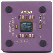
The AMD Duron was released in the summer of 2000 as a low-cost alternative to the Athlon processor and the Pentium III and Celeron processor lines from Intel. The Duron is pin-compatible with the Athlon and operating on the same motherboards. It has the same 128K of level 1 cache as the Athlon, but only 64K of level 2 cache, as compared to 256K on the more expensive chip. Because of this, the Duron generally lags behind the Athlon on business applications, but keeps up in floating-point operations thanks to its powerful FPU, which is identical to the Athlons. The original Duron was limited to operating on a 100 MHz front-side bus speed, while the Athlon at the time could run on a bus clock of 133 MHz. Later Athlons supported a 200MHz bus.

AMD K6-2plus
AMD K6-2plus
📅 2000
Ficha técnica

Historia

The K6-2+ is a revised version of the K6-III. Essentially, the K6-2+ is a K6-III with a 128 KB L2 cache made on a new 180nm production process. It was also the first processors to be available with the PowerNow! power saving technology. Essentially, the power savings were achieved with a combination of frequency (through adjusting multipliers) and voltage reduction.

IBM Gekko
IBM Gekko
📅 2000
Ficha técnica

Historia

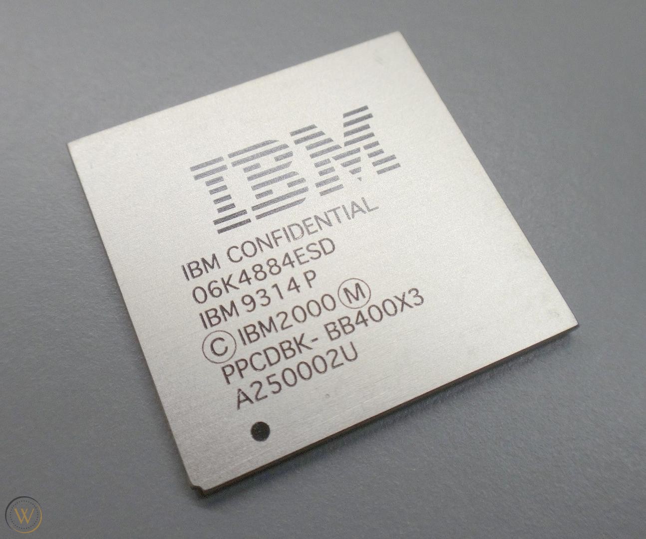
Gekko is a superscalar out-of-order 32-bit PowerPC microprocessor custom-made by IBM in 2000 for Nintendo to use as the CPU in their sixth generation game console, the Nintendo GameCube, and later the Triforce Arcade Board. Gekkos role in the game system was to facilitate game scripting, Artificial Intelligence, physics and collision detection, custom graphics lighting effects and geometry such as smooth transformations, and moving graphics data through the system. The project was announced in 1999 when IBM and Nintendo agreed to a one billion dollar contract for a CPU running at approximately 400 MHz. IBM chose to modify their existing PowerPC 750CXe processor to suit Nintendos needs, such as tight and balanced operation alongside the Flipper graphics processor. The customization was to the bus architecture, DMA, compression and floating point unit which support a special set of SIMD instructions. The CPU made ground work for custom lighting and geometry effects and could burst compressed data directly to the GPU.[citation needed] The Gekko is considered to be the direct ancestor to the Broadway processor, also designed and manufactured by IBM, that powers the Wii console.

Intel Pentium 4
Intel Pentium 4
📅 2000
Ficha técnica

Historia

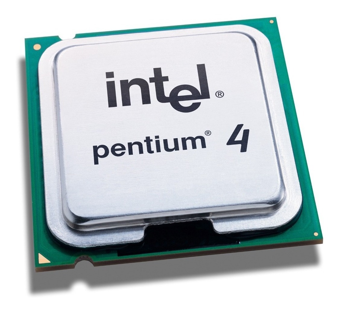
Intel Pentium 4 is a family of high-performance microprocessors that succeeded Pentium III family. Pentium 4 CPUs are based on new NetBurst micro-architecture, which differed significantly from P6 micro-architecture used in Pentium II/Pentium III microprocessors. As an overall CPU performance is proportional to its frequency and its efficiency, to achieve better performance levels many micro-architectures, including P6, strike a delicate balance between faster CPU frequencies and improved efficiency.

Intel Pentium III Celeron
📅 2000
Ficha técnica

Historia

Second generation Celeron, based on the Pentium III. The Celeron family is a line of budget x86 processors based on Pentium P6 designs. It is marketed by Intel as a second line to complement their more expensive but higher-performance Pentium CPUs. The first Celeron was introduced in April 1998 and based on the Pentium II. Later versions are based on the Pentium III and Pentium 4 designs. The Celeron product concept was introduced by Intel in response to the companys loss of low-end market share, in particular to Cyrixs 6x86 and AMDs K6, but also to other competers such as the IDT Winchip. Intels venerable Pentium MMX was no longer performance competitive and although a faster Pentium MMX would be cheap to make and technically straightforward, Intel preferred to move away from the industry standard Socket 7 platform (for which competitors made drop-in replacement CPUs) and produced a budget part that was pin-compatible with their high-end Pentium II product (Slot 1). For both technical and legal reasons, competitors had difficulty making Slot 1 parts. References: Intel Celeron Processor Home

Intel Pentium III Xbox
📅 2000
Ficha técnica

Historia

A modified version of Coppermine was developed for Microsofts Xbox game console. The only significant change was that the chip lost half of its L2 cache, dropping it down to 128 KB. Unlike the Celeron Coppermine variant with the same size L2 cache, Xboxs Coppermine core kept all of its 8-way L2 cache associativity from the Pentium III. This meant that the Xbox CPUs L2 cache was more efficient than Celerons. The Xbox CPU was manufactured onto the same Micro-PGA2 packaging as notebook chips.

VIA Cyrix III
VIA Cyrix III
📅 2000
Ficha técnica

Historia

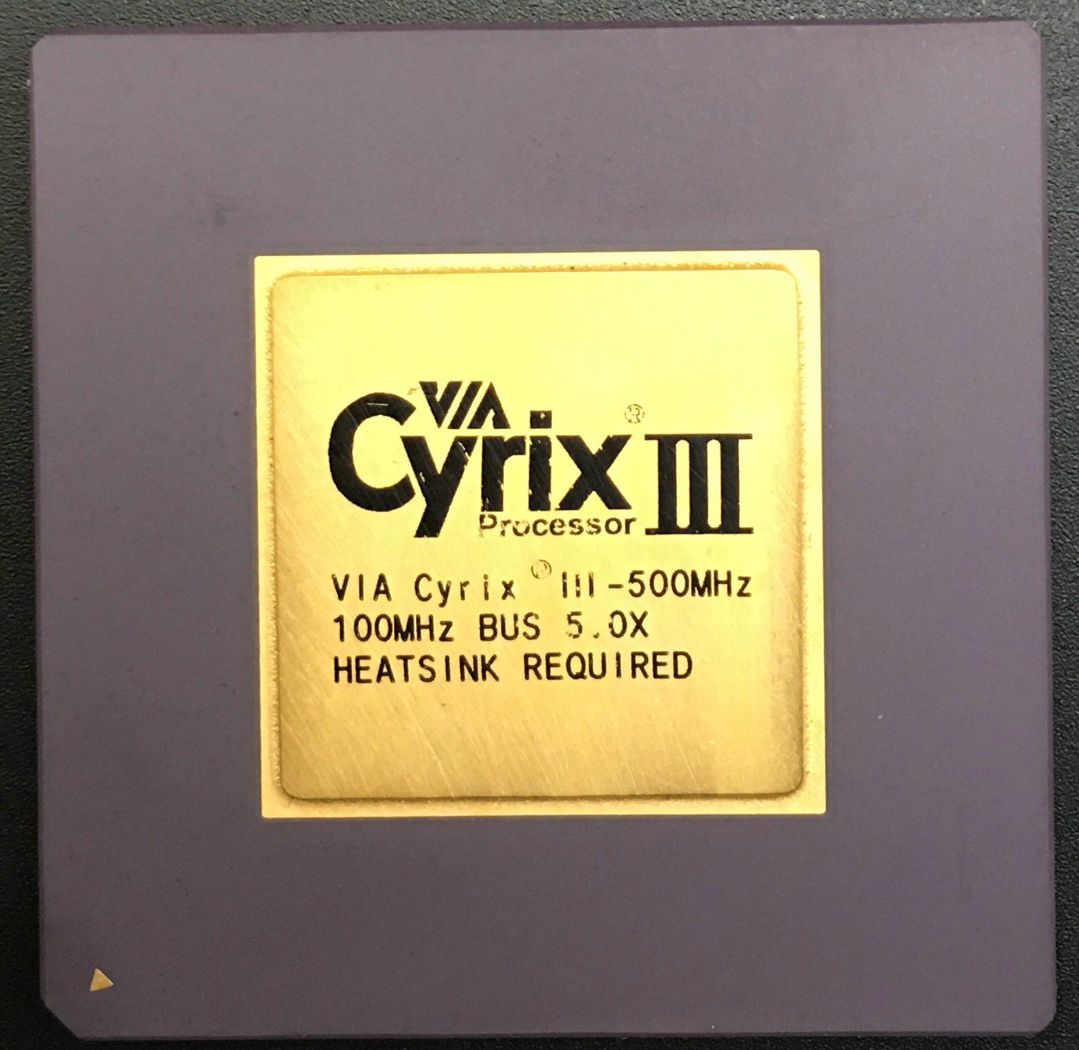
Cyrix III is an x86-compatible Socket 370 CPU. VIA Technologies launched the processor in February 2000. VIA had purchased both Centaur Technology and Cyrix. Cyrix III was to be based upon a core from one of the two companies.

Intel Pentium III Tualatin
📅 2001
Ficha técnica

Historia

The third Pentium III-version, Tualatin, was really just a trial for Intels new 0.13 �m process. As the Pentium 4 had a much bigger die size than the Pentium III, Intel would get more usable Pentium IIIs out of a wafer, and this would allow them to introduce the 0.13 �m Pentium 4 (Northwood) once the process was achieving optimal yields. Tualatin performed quite well, especially in variations which had 512 KiB L2 cache (called the Pentium III-S). The Pentium III-S variant was mainly intended for servers, especially those where power consumption mattered, i.e., thin blade servers. Pentium III Tualatins were released during 2001 until early 2002 at speeds of 1.0, 1.13, 1.2, 1.26, 1.33 and 1.4 GHz. Intel did not want a repeat of the situation where the performance of a lower priced Celeron rivaled that of the more expensive Pentium II, so Tualatin never ran faster than 1.4 GHz, the introductory clock rate of the Pentium 4. Overclockers discovered as well that 1.4-1.5 GHz with air-cooled temperatures was reaching the limits of the process and so Intel may have also wanted to avoid sacrificing profits with lower yields of a faster chip. The Tualatin core was named after the Tualatin Valley and Tualatin River in the Oregon area. Tualatins can be visually distinguished from Coppermine-based Pentium IIIs by the metal heatspreader fixed on top of the package.

VIA C3
VIA C3
📅 2001
Ficha técnica

Historia

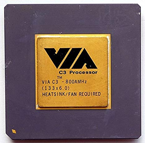
The VIA C3 is a family of x86 central processing units for personal computers designed by Centaur Technology and sold by VIA Technologies. The different CPU cores are built following the design methodology of Centaur Technology. In addition to x86 instructions, VIA C3 CPUs contain an undocumented Alternate Instruction Set allowing lower-level access to the CPU and in some cases privilege escalation.

VIA C7
VIA C7
📅 2005
Ficha técnica

Historia

The VIA C7 is an x86 central processing unit designed by Centaur Technology and sold by VIA Technologies The C7 delivers a number of improvements to the older VIA C3 cores but is nearly identical to the latest VIA C3 Nehemiah core. The C7 was officially launched in May 2005, although according to market reports, full volume production was not in place at that date. In May 2006 Intels cross-licensing agreement with VIA expired and was not renewed, which was the reason for the forced termination of C3 shipments on March 31, 2006, as VIA lost rights to the socket 370. The C7 appears still to be found in the marketplace, for example, on the bargain-priced Everex TC2502, sold by Walmart with a Linux distribution preinstalled and on the HP Mini-Note.

IBM Broadway
IBM Broadway
📅 2006
Ficha técnica

Historia

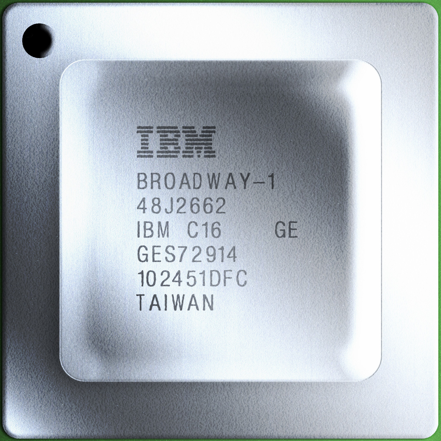
Broadway is the codename of the 32-bit Central Processing Unit (CPU) used in Nintendos Wii video game console. It was designed by IBM, and was initially produced using a 90nm SOI process and later produced with a 65nm SOI process. According to IBM, the processor consumes 20% less power than its predecessor, the 180 nm Gekko used in the Nintendo GameCube video game console.[1] Broadway was produced by IBM at their 300 mm semiconductor development and manufacturing facility in East Fishkill, New York. The bond, assembly, and test operation for the Broadway module is performed at the IBM facility in Bromont, Quebec. Very few official details have been released to the public by Nintendo or IBM. Unofficial reports claim it is derived from the 486 MHz Gekko architecture used in the GameCube and runs 50% faster at 729 MHz.[2] The PowerPC 750CL, released in 2006, is a stock CPU offered by IBM and virtually identical to Broadway. The only difference is that the 750CL came in variants, ranging from 400 MHz up to 1000 MHz

VIA Nano
VIA Nano
📅 2008
Ficha técnica

Historia

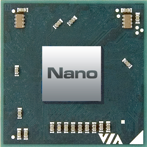
The VIA Nano (formerly code-named VIA Isaiah) is a 64-bit CPU for personal computers. The VIA Nano was released by VIA Technologies in 2008 after five years of development[1] by its CPU division, Centaur Technology. Unlike Intel and AMD, VIA uses two distinct development code names for each of its CPU cores. In this case, the codename CN was used in the United States by Centaur Technology. Biblical names are used as codes by VIA in Taiwan, and Isaiah was the choice for this particular processor and architecture. It is expected that the VIA Isaiah will be twice as fast in integer performance and four times as fast in floating-point performance as the previous-generation VIA Esther at an equivalent clock speed. Power consumption is also expected to be on par with the previous-generation VIA CPUs, with thermal design power ranging from 5 W to 25 W.

Federico Faggin
Federico Faggin
🌍 Italia
Ficha técnica

Historia

Federico Faggin (born 1 December 1941) is an Italian physicist, engineer, inventor and entrepreneur. He is best known for designing the first commercial microprocessor, the Intel 4004. He led the 4004 (MCS-4) project and the design group during the first five years of Intels microprocessor effort. Faggin also created, while working at Fairchild Semiconductor in 1968, the self-aligned MOS (metal–oxide–semiconductor) silicon-gate technology (SGT), which made possible MOS semiconductor memory chips, CCD image sensors, and the microprocessor. After the 4004, he led development of the Intel 8008 and 8080, using his SGT methodology for random logic chip design, which was essential to the creation of early Intel microprocessors. He was co-founder (with Ralph Ungermann) and CEO of Zilog, the first company solely dedicated to microprocessors, and led the development of the Zilog Z80 and Z8 processors. He was later the co-founder and CEO of Cygnet Technologies, and then Synaptics.

Hitachi HD38800
Hitachi HD38800
Ficha técnica

Historia

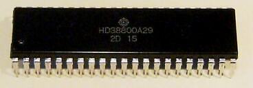
Hitachi Semiconductor PMOS 4-Bit Single Chip Microcomputer

Hitachi HD38820
Hitachi HD38820
Ficha técnica

Historia

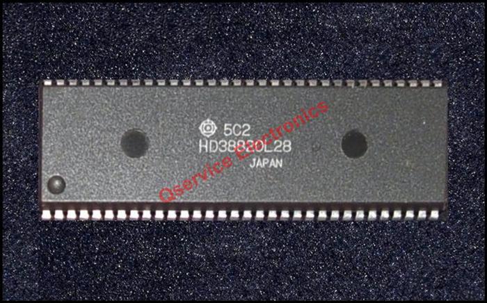
Hitachi IC HD-38820-L28, VTR Custom 4-Bit Microprocessor HD 38820-L28

National Semiconductor COP444L
Ficha técnica

Historia

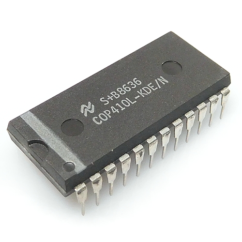
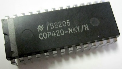
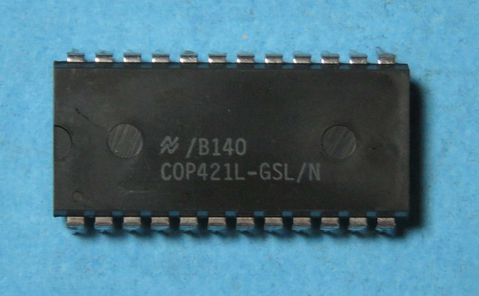
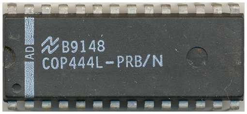
The COP444L is one model of a family of microcontrollers from National Semiconductor. It has 2K of 8-bit ROM and 128 4-bit nibbles of RAM. One handheld game that used it is Entex Space Invader. It can be electronically dumped.
Philips SCC68070
Philips SCC68070
Ficha técnica

Historia

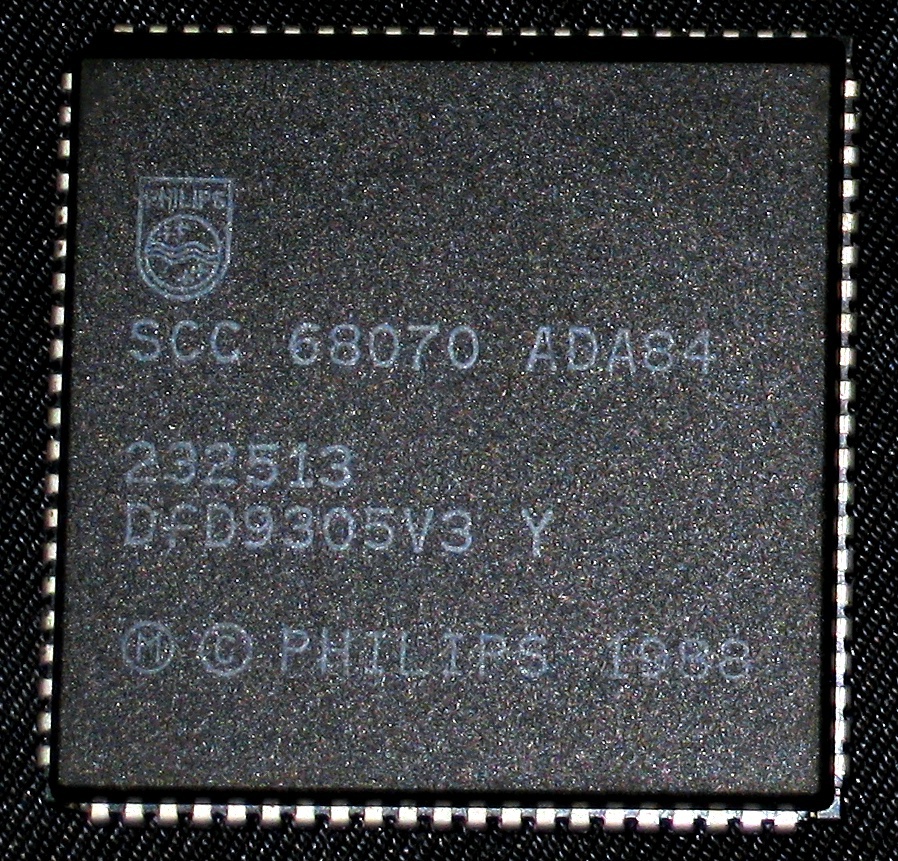
The SCC68070 is a Philips Semiconductors-branded, Motorola 68000-based 16/32-bit processor produced under license. While marketed externally as a high-performance microcontroller, it has been almost exclusively used combined with the Philips SCC66470 VSC (Video- and Systems Controller) in the Philips CD-i interactive entertainment product line.

Sharp SM510
Sharp SM510
Ficha técnica

Historia

Sharp SM510: ROM 2772×8 bit, RAM 128×4 bit, a divider and 132-segment LCD driver circuit

Página 3 de 4